Related news by tag Nanooptics
María Barra receives the Nanolito award for her Doctoral Thesis

The diplomas accrediting the Nanolito Doctoral Thesis Awards have been presented at the XXXIX Biennial of the Royal Spanish Society of Physics (RSEF), which is being held these days in Donostia San Sebastian. These awards seek to highlight the contribution of young scientists to the fields of nanolithography and nanofabrication, specifically those who have recently defended their doctoral thesis in Spain.
nanoGUNE research appears on Nature Photonics cover
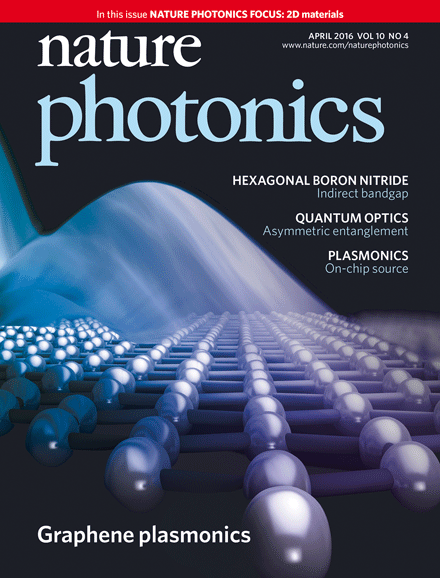
The work has been published by Nature Photonics (see https://www.nanogune.eu/newsroom/nanolight-edge) and now appeared on the cover of the april 2016 issue.
Nature Materials: Graphene plasmons go ballistic
This problem has now been solved, as shown by researchers from ICFO (Barcelona), in a collaboration with nanoGUNE, CNR/Scuola Normale Superiore (Pisa, Italy) – members of the EU Graphene Flagship – and Columbia University (New York, USA).
 Since the discovery of graphene, many other two-dimensional materials have been isolated in the laboratory. One example is boron nitride, a very good insulator. A combination of these two unique two-dimensional materials has provided the solution to the quest for controlling light in tiny circuits and suppression of losses. When graphene is encapsulated in boron nitride, electrons can move ballistically for long distances without scattering, even at room temperature. This new research shows that the graphene/boron nitride material system is also an excellent host for extremely strongly confined light and suppression of plasmon losses.
The research, carried out by ICFO PhD students Achim Woessner and Yuando Gao and postdoctoral fellow Mark Lundeberg, is just the beginning of a series of discoveries on nano-optoelectronic properties of new heterostructures based on combining different kinds of two-dimensional materials. The material heterostructure was first discovered by the researchers at Columbia University.
Ikerbasque Professor Rainer Hillenbrand, nanoGUNE’s Nanooptics group leader, comments: “Now we can squeeze light and at the same time make it propagate over significant distances through nanoscale materials. In the future, low-loss graphene plasmons could make signal processing and computing much faster, and optical sensing more efficient.”
The research team also performed theoretical studies. Marco Polini, from CNR/Scuola Normale Superiore (Pisa) and the IIT Graphene Labs (Genova, Italy), laid down a theory and performed calculations together with their collaborators.
These findings pave the way for extremely miniaturized optical circuits and devices that could be useful for optical and/or biological sensing, information processing or data communications.
Original Publication
A. Woessner,M. B. Lundeberg, Y. Gao, A. Principi, P. Alonso-González, M. Carrega, K. Watanabe, T. Taniguchi, G. Vignale, M. Polini, J. Hone, R. Hillenbrand, and F. H. L. Koppens
Nature Materials (2014) Highly confined low-loss plasmons in graphene–boron nitride heterostructures
Nano-scale molecular detective: New on-chip device uses exotic light rays in 2D material to detect molecules
 enhance the molecular fingerprint signal encoded in the photocurrent. (Credit: Dr. David Alcaraz, ICFO)")
Molecules have some sort of fingerprints, unique features that can be used to differentiate them. Each type of molecule, when illuminated with the right light, vibrates at a characteristic frequency (its resonance frequency, which typically occurs at infrared frequencies) and strength. Similar to what can be done with human fingerprints, one can exploit this information to distinguish different types of molecules or gases from each other.
The CENTINELA project, a winner in the Inspire programme

The CENTINELA project is seeking to develop a system of remote detection that can be used as a basis for the detection and early warning of substances responsible for unpleasant odours in the environs of the refinery. The project has been specifically designed to address the basic needs raised by Petronor.
The detection systems will be developed at the facilities of the CFM/MPC and nanoGUNE and will later be transferred to the University of Burgos where its laboratories are equipped to work on samples of chemical substances in safe conditions. During the final phase, the equipment will be moved to the Petronor facilities for field testing.
Tasks of each principal member
The participant and the collaborators will be carrying out the following functions:
- CFM/MPC (Project and Innovation Management Unit): This is responsible for the work to manage and coordinate the project. It will be participating in the work to define the specifications, design the software and measuring systems, and develop the measuring and pre-industrial-scale production systems.
- CIC nanoGUNE (Nanooptics Group): It is set to participate in developing the measuring systems (Fourier transform spectrometer, optical design, signal processing) and the characterising of them.
- University of Burgos (Instrumental Analysis Group): It will be gathering the spectroscopic data on the substances responsible for the unpleasant odours, characterising the measuring instrument, and developing the multivariate analysis software for automatic detection and early warning.
- Petronor: It will be responsible for the general monitoring of progress. Specification of requirements. Mapping of substance types and potential emission zones.
CIC nanoGUNE´s research on light covered in Nature Photonics

Light plays an essential role in modern science and technology, with applications ranging from fast optical communication to medical diagnosis and laser surgery. In many of these applications, the interaction of light with matter is of fundamental importance.
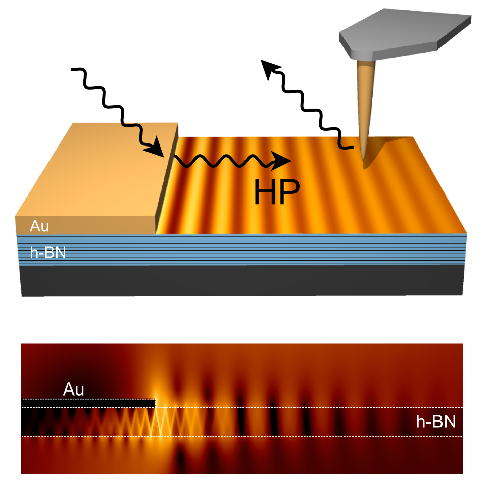
On-chip observation of THz graphene plasmons
Radiation in the terahertz (THz) frequency range is attracting large interest because of its manifold application potential for non-destructive imaging, next-generation wireless communication or sensing. But still, the generating, detecting and controlling of THz radiation faces numerous technological challenges. Particularly, the relatively long wavelengths (from 30 to 300 μm) of THz radiation require solutions for nanoscale integration of THz devices or for nanoscale sensing and imaging applications.
In recent years, graphene plasmonics has become a highly promising platform for shrinking THz waves. It is based on the interaction of light with collective electron oscillations in graphene, giving rise to electromagnetic waves that are called plasmons. The graphene plasmons propagate with strongly reduced wavelength and can concentrate THz fields to subwavelength-scale dimensions, while the plasmons themselves can be controlled electrically.
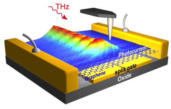
Now, researchers at CIC nanoGUNE (San Sebastian, Spain) in collaboration with ICFO (Barcelona, Spain), IIT (Genova, Italy) - members of the EU Graphene Flagship - Columbia University (New York, USA), Radboud University (Nijmegen, Netherlands), NIM (Tsukuba, Japan) and Neaspec (Martinsried, Germany) could visualize strongly compressed and confined THz plasmons in a room-temperature THz detector based on graphene. To see the plasmons, they recorded a nanoscale map of the photocurrent that the detector produced while a sharp metal tip was scanned across it. The tip had the function to focus the THz illumination to a spot size of about 50 nm, which is about 2000 times smaller than the illumination wavelength. This new imaging technique, named THz photocurrent nanoscopy, provides unprecedented possibilities for characterizing optoelectronic properties at THz frequencies.
The team recorded photocurrent images of the graphene detector, while it was illuminated with THz radiation of around 100 μm wavelength. The images showed photocurrent oscillations revealing that THz plasmons with a more than 50 times reduced wavelength were propagating in the device while producing a photocurrent.
“In the beginning we were quite surprised about the extremely short plasmon wavelength, as THz graphene plasmons are typically much less compressed”, says former nanoGUNE researcher Pablo Alonso, now at the University of Oviedo, and first author of the work. “We managed to solve the puzzle by theoretical studies, which showed that the plasmons couple with the metal gate below the graphene”, he continues. “This coupling leads to an additional compression of the plasmons and an extreme field confinement, which could open the door towards various detector and sensor applications”, adds Rainer Hillenbrand, Ikerbasque Research Professor and Nanooptics Group Leader at nanoGUNE who led the research. The plasmons also show a linear dispersion – that means that their energy is proportional to their momentum - which could be beneficial for information and communication technologies. The team also analysed the lifetime of the THz plasmons, which showed that the damping of THz plasmons is determined by the impurities in the graphene.
THz photocurrent nanoscopy relies on the strong photothermoelectric effect in graphene, which transforms heat generated by THz fields, including that of THz plasmons, into a current. In the future, the strong thermoelectric effect could be also applied for on-chip THz plasmon detection in graphene plasmonic circuits. The technique for THz photocurrent nanoimaging could find further application potential beyond plasmon imaging, for example, for studying the local THz optoelectronic properties of other 2D materials, classical 2D electron gases or semiconductor nanostructures.
Understanding nanolight refraction on highly anisotropic materials

Light refraction accounts for the change of direction and speed that a wave undergoes when passing from one medium to another. Glasses and contact lenses, microscopes and telescopes, or something as commonplace as the fact that a pencil inserted into a glass of water appears bent when viewed from the outside, have their origin in the optical phenomenon of refraction.
Basque researchers turn light upside down

Scientists had already theoretically predicted that specifically structured surfaces can turn the wavefronts of light upside down when it propagates along them. "On such surfaces, called hyberbolic metasurfaces, the waves emitted from a point source propagate only in certain directions and with open (concave) wavefronts", explains Javier Alfaro, PhD student at nanoGUNE and co-author of the paper. These unusual waves are called hyperbolic surface polaritons. Because they propagate only in certain directions, and with wavelengths that are much smaller than that of light in free space or standard waveguides, they could help to miniaturize optical devices for sensing and signal processing.
Now, the researchers developed such a metasurface for infrared light. It is based on boron nitride, a graphene-like 2D material, and was selected because of its capability to manipulate infrared light on extremely small length scales, which could be applied for the development of miniaturized chemical sensors or for heat management in nanoscale optoelectronic devices. On the other hand, the researchers succeeded to directly observe the concave wavefronts with a special optical microscope, which have been elusive so far.
Hyperbolic metasurfaces are challenging to fabricate because an extremely precise structuring on the nanometer scale is required. Irene Dolado, PhD student at nanoGUNE, and Saül Vélez, former postdoctoral researcher at nanoGUNE (now at ETH Zürich) mastered this challenge by electron beam lithography and etching of thin flakes of high-quality boron nitride provided by Kansas State University. "After several optimization steps, we achieved the required precision and obtained grating structures with gap sizes as small as 25 nm”, Dolado says. “The same fabrication methods can also be applied to other materials, which could pave the way to realize artificial metasurface structures with custom-made optical properties”, adds Saül Vélez.
To see how the waves propagate along the metasurface, the researchers used a state-of the-art infrared nanoimaging technique that was pioneered by the nanoptics group at nanoGUNE. They first placed an infrared gold nanorod onto the metasurface. “It plays the role of a stone dropped into water”, says Peining Li. The nanorod concentrates incident infrared light into a tiny spot, which launches waves that then propagate along the metasurface. With the help of a so-called scattering-type scanning near-field microscope (s-SNOM) the researchers imaged the waves. “It was amazing to see the images. They indeed showed the concave curvature of the wavefronts that were propagating away form the gold nanorod, exactly as predicted by theory“, says Rainer Hillenbrand, Ikerbasque Professor at nanoGUNE, who led the work.
The results promise nanostructured 2D materials to become a novel platform for hyberbolic metasurface devices and circuits, and further demonstrate how near-field microscopy can be applied to unveil exotic optical phenomena in anisotropic materials and for verifying new metasurface design principles.
The research has been mainly funded by individual fellowship grants of the European Union Marie Sklodowsca-Curie Actions and the pre-doctoral research grants program of the Basque and Spanish Governments, as well as by the National Science Foundation (USA), and has been carried out in line with nanoGUNEs projects within the EU's Graphene Flagship.
Review: Nanoscale terahertz scanning probe microscopy

Terahertz radiation has become an important diagnostic tool in the development of new technologies. However, the diffraction limit prevents terahertz radiation (λ ≈ 0.01–3 mm) from being focused to the nanometer length scale of modern devices. In response to this challenge, terahertz scanning probe microscopy techniques based on coupling terahertz radiation to subwavelength probes such as sharp tips have been developed.
Students from UPV / EHU, Tecnun, UAB and the UB carry out summer internships at CIC nanoGUNE
On Tuesday, 19 June, we welcomed a group of internship students that will carry out a research project at NanoGUNE during the summer. The director of the center, Jose M. Pitarke, received the students with a presentation talk about nanoGUNE, that was also attended by the researchers that will conduct the students’ projects.
The 11 students come from different universities, among which are, Unibersity of the Basque Country (UPV /EHU), Tecnun, Univeristy of Barcelona (UB), Autonomous University of Barcelona (UAB). This program offers to the students a real experience of work in a research laboratory in order to make it easier for them to take decision about their future professional life.
The students will collaborate and learn with the different research groups at nanoGUNE, such as nanooptics, nanodevices or nanomagnetism. They will carry out a research project for two months following the instructions of a researcher of their group.
Some of them started the internships at the beginning of the month and they have been very involved in the group’s work. "The truth is that we started very suddenly; the very first day they took me to the laboratory," says Amaia Ochandorena, a student of Biochemistry and Molecular Biology at the UPV/EHU.
All the students knew CIC nanoGUNE and stressed that "it is an important research center" and "offers and works with topics of much interest".
For these students, and also for undergraduate students of general, nanoGUNE offers the possibility of collaborating with the center for the completion of final graduate or master thesis projects, for which also opens a call for grants every year.
Review: Interface nano-optics with van der Waals polaritons
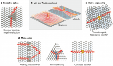
Polaritons are hybrid excitations of matter and photons. In recent years, polaritons in van der Waals nanomaterials—known as van der Waals polaritons—have shown great promise to guide the flow of light at the nanoscale over spectral regions ranging from the visible to the terahertz. A vibrant research field based on manipulating strong light–matter interactions in the form of polaritons, supported by these atomically thin van der Waals nanomaterials, is emerging for advanced nanophotonic and opto-electronic applications.
Pablo Alonso-González, Winner of the RSEF-BBVA Foundation 2014 prize
After getting his PhD, he began to work as a post-doctoral researcher in the Nanooptics group of nanoGUNE led by the Ikerbasque researcher Rainer Hillenbrand, where he is now doing his research work. Some of his pieces of work on the optical properties of nanoscale graphene have been published in journals of major international prestige like Nature and Science. In an article recently published in Science, he showed experimentally that confined nanoscale light in graphene obeys the laws of conventional optics, which constitutes the first step towards the development of two-dimensional nanooptics.
RSEF-BBVA Foundation Awards for Physics [www.resef.es]
The Royal Spanish Society for Physics (RSEF), founded in 1903, began to award these prizes in 1958 to recognize creativity and effort and to encourage researchers, young ones in particular. The awards are divided into the following sections: The RSEF Medal, totalling 15,000 euros; New Researcher, in two categories, Theoretical Physics and Experimental Physics, each worth 4,000 euros; Physics Education and Popularisation in two categories, University Education and Secondary Education (8,000 euros each); Physics, Innovation and Technology (8,000 euros); Best Papers in RSEF publications (two prizes, one for education and the other for research, each worth 1,500 euros). The BBVA Foundation has been collaborating with the RSEF since 2007 in these prizes which are awarded every year.
nanoGUNE launches a new summer internship call for university students
Through this programme the Basque nanoscience research centre will this summer be receiving about ten new students in their 3rd and 4th years of Physics, Chemistry, Biology and Engineering. For a period of six weeks or two months the young students will be collaborating with nanoGUNE researchers in their research projects on subjects such as electron/spin phenomena and magnetism, nanoscale optics, nanoscale materials and nanobioengineering, among others.
To participate in the summer internship programme any students who are interested will need to submit their applications online via the nanoGUNE website, the deadline being 16 February. Full information relating to the call is available via the nanoGUNE website (www.nanogune.eu)
Researchers develop an innovative strategy to focus infrared light into the nanoscale
")
Focusing of light into the nanoscale represents a landmark for the implementation of nanotechnology in optics and biochemistry. Based on the exotic propagation of light in highly anisotropic materials (where light propagates in the form of rays along specific directions), a research team led by the University of Oviedo has demonstrated the focusing of infrared light into extraordinarily small regions.
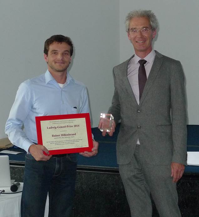
The Ludwig-Genzel-Prize 2014 is awarded to Rainer Hillenbrand
Rainer Hillenbrand received the award from the hands of Prof. Dressel, chairman of the selection committee, during the LEES 2014 conference in Loire Valley (France) for his pioneering and world-leading developments in the field of optical near-field microscopy. Hillenbrand studied at the University of Augsburg and developed his PhD research at the Max-Planck Institute of Biochemistry in Martinsried, both in Germany. During his PhD, Hillenbrand and his colleagues developed a novel scanning near-field optical microscope for background-free amplitude and phase resolved optical imaging with nanoscale spatial resolution, which they named scattering-type scanning near-field microscopy (s-SNOM). This development was a breakthrough in the field and inspired many groups worlwide to start working in this direction. He continued working at the same German institute and built up his own independent junior research group. Further developments made possible to found the start-up company Neaspec in 2007, which has been the first company offering commercial s-SNOM systems.
In 2008, Hillenbrand joined nanoGUNE as the group leader of the Nanooptics group and Ikerbasque Research Professor. He has applied his technique to perform cutting-edge research in different fields, including fundamental solid-state physics, materials science, life science, and nanophotonics. Recent developments include nanoscale infrared Fourier transform spectroscopy (nano-FTIR), which enables infrared spectroscopy with a more than 100 times improved spatial resolution compared to conventional infrared spectroscopy systems. Hillenbrand currently applies the techniques for chemical identification of nanomaterials, protein studies and the development of graphene-based nanophotonics.
According to the price committee, the revolutionary surface-imaging technique allows to perform spectrally resolved measurements from the visible to the microwave regime with an unprecedented spatial resolution. Hillenbrand work “reveals a unique combination of engineering skills and deep insights into the scientific problems of the various topics, addressing both fundamental questions and applications reaching all the way to industrial maturity”.
Ludwig-Genzel-Prize
The Ludwig-Genzel-Prize is awarded to a young scientist for exceptional contributions to the field of condensed-matter spectroscopy. Related to Ludwig Genzel’s scientific oeuvre the focus is on the far-infrared spectral range. The award contains a diploma and prize money of 4000 €. Bruker Optics (Ettlingen) is the sponsor of this prize. The prize is awarded every two years during the International Conference on Low Energy Electrodynamics in Solids (LEES). The selection is made by a committee. The current members of the selection committee are: Martin Dressel —chairman— (Univ. Stuttgart, Germany), Leonardo Degiorgi (EHT Zürich, Switzerland), Jan Petzelt (Academy of Sciences, Praha, Czech Republic), Karl Renk (Univ. Regensburg, Germany) and Hartmut Roskos (Univ. Frankfurt, Germany).
How to manipulate light on the nanoscale over wide frequency ranges

Research with nanolight based on phonon polaritons has developed considerably in recent years thanks to the use of sheet-structured nanomaterials such as graphene, boron nitride or molybdenum trioxide: the so-called van der Waals materials. Nanolight based on phonon polaritons is very promising because it can live longer than other forms of nanolight, but one of the main drawbacks to the technological applications of this nanolight based on phonon polaritons is the limited frequency ranges characteristic of each material, it exists only in narrow frequency region.
But now, an international team has proposed a novel method that allows to widely extend this range of working frequencies of phonon polaritons in van der Waals materials. This consists in the intercalation of alkaline and alkaline earth atoms, such as sodium, calcium or lithium, in the laminar structure of the van der Waals vanadium pentaoxide material, thus allowing to modify its atomic bonds and consequently its optical properties.
Considering that a large variety of ions and ion contents can be intercalated in layered materials, on-demand spectral response of phonon polaritons in van der Waals materials can be expected, eventually covering the whole mid-infrared range, something critical for the emerging field of phonon polariton photonics.
The finding, published in the journal Nature Materials, will allow progress in the development of compact photonic technologies, such as high-sensitivity biological sensors or information and communication technologies at the nanoscale.
Registration period for the summer internship program open
CIC nanoGUNE has just launched the program for summer internships, which runs every year. University students are offered the chance to get involved in the activity of a world-class research center.
Infrared sheds light on single protein complexes
Proteins are basic building blocks of life. The chemistry and structure of proteins are essential for their biological function. Indeed, the structure of proteins determines their mechanical and catalytic properties (e.g. enzymes). Such functions literally shape all living beings. Furthermore, the protein structure also plays a major role in many diseases. For example, the secondary structure of a protein (whether it has helical (alpha-) or sheet-like (beta-) internal substructures) is highly relevant in the pathogenous mechanism leading to Alzheimer, Parkinson, and other neuro-degenerative diseases. Although a variety of methods have been developed to study the protein chemistry and structure, recognizing and mapping the secondary structure on the nanometer scale, or even with single protein sensitivity, is still a major challenge. A new infrared spectroscopy technique, called nano-FTIR, has now enabled nanoscale chemical imaging and probing of protein’s secondary structure with enormous sensitivity.
nano-FTIR is an optical technique that combines scattering-type scanning near-field optical microscopy (s-SNOM) and Fourier transform infrared (FTIR) spectroscopy. The latter is a tool often used for studying secondary structure of proteins that, however, does not allow for nanoscale mapping of proteins by itself. In nano-FTIR, a sharp metalized tip is illuminated with a broadband infrared laser beam, and the backscattered light is analyzed with a specially designed Fourier transform spectrometer. With this technique, the researchers could now demonstrate local infrared spectroscopy of proteins with a spatial resolution of less than 30 nm.
“The tip acts as an antenna for infrared light and concentrates it at the very tip apex. The nanofocus at the tip apex can be thus considered as an ultra-small infrared light source. It is so small that it only illuminates an area of about 30×30 nm, which is the scale of large protein complexes”, says project leader Rainer Hillenbrand.
In order to demonstrate the versatility of nano-FTIR for nanoscale-resolved protein spectroscopy, the researchers measured infrared spectra of single viruses, ferritin complexes, purple membranes and insulin fibrils. “They all exhibit variations of their secondary structure – describes Iban Amenabar, who performed the nanospectroscopy experiments-; viruses and ferritin are mainly made of alpha-helical structures, while insulin fibrils are mainly made of beta-sheet structures”. Simon Poly, the biologist in the team, explains that “in a mixture of insulin fibrils and few viruses, standard FTIR spectroscopy did not reveal the presence of the alpha-helical viruses. By probing the protein nanostructures one by one with nano-FTIR we could clearly identify the virus, that is the alpha-helical structures within the beta-sheet ones”.
An important aspect of enormous practical relevance is that the nano-FTIR spectra of proteins match extremely well with conventional FTIR spectra, while the spatial resolution is increased by more than 100. “We could measure infrared spectra of even single ferritin particles. These are protein complexes of only 24 proteins. The mass of one ferritin complex is extremely small, only 1 attogram, but we could clearly recognize its alpha-helical structure”, says Amenabar.
The researchers also studied single insulin fibrils, which are a model system for neurodegenerative diseases. It is known that insulin fibrils have a core of beta-sheet structure but their complete structure is still not fully clarified. “In nano-FTIR spectra of individual fibrils we recognized not only beta-sheet structure, but also alpha-helical structures, which might be of relevance for fibril association,” says Alexander Bittner, leader of the Self-Assembly Group at nanoGUNE.
“We are excited about the novel possibilities that nano-FTIR offers. With sharper tips and improved antenna function, we also hope to obtain infrared spectra of single proteins in the future. We see manifold applications, such as studies of conformational changes in amyloid structures on the molecular level, the mapping of nanoscale protein modifications in biomedical tissue or the label-free mapping of membrane proteins. This could lead to a new era in infrared nano-bio-spectroscopy”, concludes Rainer Hillenbrand, head of the Nanooptics Group at nanoGUNE.
Original publication
I. Amenabar, S. Poly, W. Nuansing, E. H. Hubrich, A. A. Govyadinov, F. Huth, R. Krutokhvostov, L. Zhang, M. Knez, J. Heberle, A.M. Bittner and R. Hillenbrand. “Structural analysis and mapping of individual protein complexes by infrared nanospectroscopy” Nature Communications, 2013, DOI: 10.1038/ncomms3890
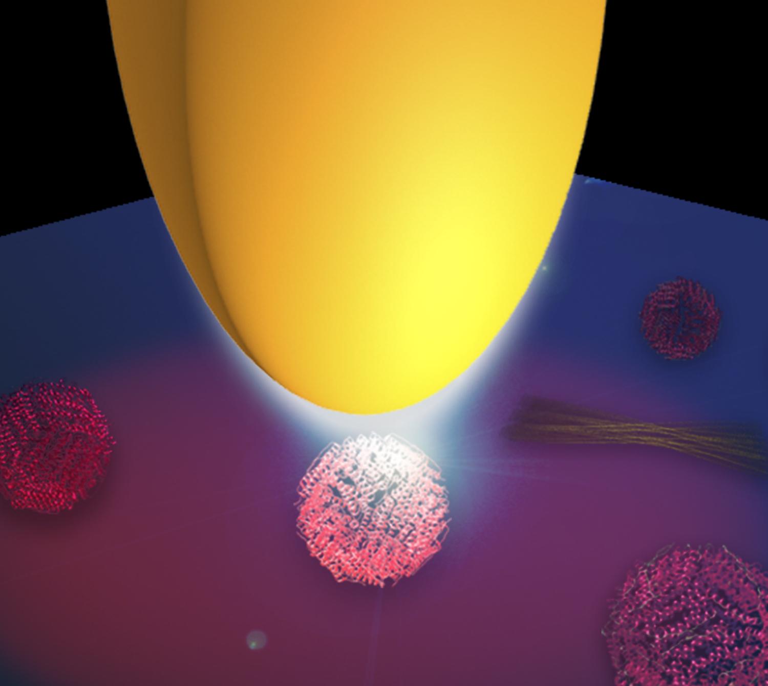
Figure: Illustration of infrared protein nano-spectroscopy. A metal tip (yellow) is illuminated with infrared light. Due the antenna function of the tip, the light is concentrated at the tip apex and creates a nanofocus, which illuminates the proteins. Copyright: CIC nanoGUNE
Nanoparticles as drug carriers

Due to their size, the physical properties of nanoparticles are very different from those of macroscopic materials, even when they have the same chemical composition. Therefore, the use of nanoparticles to administer drugs has revolutionised the fields of both nanotechnology and medicine.
'When administering a drug, in order to guarantee efficient performance, it is vital to ensure it is effectively delivered to the right place. Nanoparticles are able to store and transport drugs to the required site in an effective manner. It is best to load them with the maximum possible quantity of the drug in question, providing the particle remains stable,' explains Iban Amenabar, a researcher with nanoGUNE's Nanoóptica team. 'To do so, we obviously need techniques to enable us to measure the real quantity of the drug present in the nanoparticles. However, establishing said techniques is no easy matter,' he continues. 'Conventional measurement techniques (such as FTIR–Fourier transform infrared spectroscopy) offer limited spatial resolution and sensitivity, and only enable drug load measurements in samples containing thousands of nanoparticles. Unfortunately, this amount is not representative, since the drug may not be stored or loaded in the nanoparticles, which means it will not be transported and delivered effectively.' Thus, 'in order to determine the real, effective load, it is necessary to measure the amount of the drug in individual nanoparticles. To do this, we use the nanoscale Fourier transform infrared spectroscopy (nano-FTIR) technique, which was developed at nanoGUNE. This novel technique enables us to measure both optical images and absorption spectra with nanometric resolution and sensitivity. Specifically, the collaboration has enabled us to measure and identify drugs in individual nanoparticles for the very first time,' he adds.
The nano-FTIR technique combines the analytical capability (or chemical information) of Fournier transform infrared spectroscopy (FTIR) with the nanoscale spatial resolution of atomic force microscopy (AFM).
'As a result of the collaboration project, we were able to demonstrate the potential of the novel spectroscopy technique for analysing nanoparticles. Thanks to this technique, we can now measure and identify the drugs present in individual nanoparticles, based on the formulations developed by Kusudama Therapeutics S.L for treating various different types of lung disease,' explains Iban Amenabar.
It is important to highlight the fact that this collaboration has opened up new avenues of research aimed at ensuring greater control over nanoparticles with a wider variety of drugs.
In this particular case, the aid provided by Fomento de San Sebastián was channelled through the Technological Bonds programme, set up in collaboration with CIC nanoGUNE and other entities to promote and develop projects with a strong technological component among local companies and entrepreneurs. The programme seeks to foster the transfer of the technology and knowledge generated in research centres based in San Sebastián.
Researchers observe extremely squeezed directional THz waves in thin semiconductor crystals

Polaritons are hybrid states of light and matter that arise from the coupling of light with matter excitations. Plasmon and phonon polaritons are among the most prominent examples, formed by the coupling of light to collective electron oscillations and crystal lattice vibrations, respectively. They play a crucial role in various applications, from sub-diffraction optical spectroscopy and ultrasensitive chemical sensors to ultracompact modulators for communication applications.
Science: Flatland optics with graphene
Optical circuits and devices could make signal processing and computing much faster. “However, although light is very fast it needs too much space”, explains Rainer Hillenbrand, Ikerbasque Professor at nanoGUNE and the UPV/EHU. In fact, propagating light needs at least the space of half its wavelength, which is much larger than state-of-the-art electronic building blocks in our computers. For that reason, a quest for squeezing light to propagate it through nanoscale materials arises.
The wonder material graphene, a single layer of carbon atoms with extraordinary properties, has been proposed as one solution. The wavelength of light captured by a graphene layer can be strongly shortened by a factor of 10 to 100 compared to light propagating in free space. As a consequence, this light propagating along the graphene layer – called graphene plasmon – requires much less space.
However, transforming light efficiently into graphene plasmons and manipulating them with a compact device has been a major challenge. A team of researchers from nanoGUNE, ICFO and Graphenea – members of the EU Graphene Flagship – now demonstrates that the antenna concept of radio wave technology could be a promising solution. The team shows that a nanoscale metal rod on graphene (acting as an antenna for light) can capture infrared light and transform it into graphene plasmons, analogous to a radio antenna converting radio waves into electromagnetic waves in a metal cable.
“We introduce a versatile platform technology based on resonant optical antennas for launching and controlling of propagating graphene plasmons, which represents an essential step for the development of graphene plasmonic circuits”, says team leader Rainer Hillenbrand. Pablo Alonso-González, who performed the experiments at nanoGUNE, highlights some of the advantages offered by the antenna device: “the excitation of graphene plasmons is purely optical, the device is compact and the phase and wavefronts of the graphene plasmons can be directly controlled by geometrically tailoring the antennas. This is essential to develop applications based on focusing and guiding of light”.
The research team also performed theoretical studies. Alexey Nikitin, Ikerbasque Research Fellow at nanoGUNE, performed the calculations and explains that “according to theory, the operation of our device is very efficient, and all the future technological applications will essentially depend upon fabrication limitations and quality of graphene”.
Based on Nikitin´s calculations, nanoGUNE’s Nanodevices group fabricated gold nanoantennas on graphene provided by Graphenea. The Nanooptics group then used the Neaspec near-field microscope to image how infrared graphene plasmons are launched and propagate along the graphene layer. In the images, the researchers saw that, indeed, waves on graphene propagate away from the antenna, like waves on a water surface when a stone is thrown in.

Graphic representation of the refraction of graphene plasmons – launched by a tiny gold antenna – when passing through a one-atom-thick prism
In order to test whether the two-dimensional propagation of light waves along a one-atom-thick carbon layer follow the laws of conventional optics, the researchers tried to focus and refract the waves. For the focusing experiment, they curved the antenna. The images then showed that the graphene plasmons focus away from the antenna, similar to the light beam that is concentrated with a lens or concave mirror.
The team also observed that graphene plasmons refract (bend) when they pass through a prism-shaped graphene bilayer, analogous to the bending of a light beam passing through a glass prism. “The big difference is that the graphene prism is only two atoms thick. It is the thinnest refracting optical prism ever”, says Rainer Hillenbrand. Intriguingly, the graphene plasmons are bent because the conductivity in the two-atom-thick prism is larger than in the surrounding one-atom-thick layer. In the future, such conductivity changes in graphene could be also generated by simple electronic means, allowing for highly efficient electric control of refraction, among others for steering applications.
Altogether, the experiments show that the fundamental and most important principles of conventional optics also apply for graphene plasmons, in other words, squeezed light propagating along a one-atom-thick layer of carbon atoms. Future developments based on these results could lead to extremely miniaturized optical circuits and devices that could be useful for sensing and computing, among other applications.
Original publication
P. Alonso-González1, A.Y. Nikitin1,5, F. Golmar1,2, A. Centeno3, A. Pesquera3, S. Vélez1, J. Chen1, G. Navickaite4, F. Koppens4<, A. Zurutuza3, F. Casanova 1,5, L.E. Hueso 1,5 and R. Hillenbrand 1,5. “Controlling grapheme plasmons with resonant metal antennas and spatial conductivity patterns” Science (2014), DOI: 10.1126/science.1253202
- CIC nanoGUNE, 20018 Donostia-San Sebastián, Spain.
- I.N.T.I-CONICET and ECyT-UNSAM, San Martín, Bs. As., Argentina.
- Graphenea SA, 20018 Donostia-San Sebastián, Spain.
- ICFO-Institut de Ciéncies Fotoniques, Mediterranean Technology Park, 08860 Casteldefells, Barcelona, Spain.
- IKERBASQUE, Basque Foundation for Science, 48011 Bilbao, Spain.
CIC nanoGUNE
The nanoGUNE Cooperative Research Center, located in Donostia-San Sebastian, Basque Country, is a research centre set up with the mission to conduct excellence research into nanoscience and nanotechnology with the aim of increasing the Basque Country’s business competitiveness and economic and social development.
GRAPHENEA S.A.
Graphenea is a pioneer graphene production start-up company founded in 2010 by private investors and CIC nanoGUNE. The company produces and commercializes graphene films by Chemical Vapor Deposition technology and graphene powders by Chemical Exfoliation techniques.
ICFO
ICFO is a young research institution located in Barcelona that aims to advance the very limits of knowledge in Photonics, namely the science and technology of harnessing Light. Its research programs target the global forefront of photonics, and aim to tackle important challenges faced by society at large. ICFO is focused on current and future problems in Health, Energy, Information, Safety, Security and caring for the Environment.
Rainer Hillenbrand, new nanoGUNE Nanooptics Group Leader
Dr. Hillenbrand has a successful track record in the field of Scanning Near Field Optical Microscopy (SNOM) having developed the so-called scattering-type scanning near-field optical microscopy (s-SNOM). He was the prizewinner of the “Young Scientist Competition in Nanotechnology 2002”, awarded by the Bundesministerium für Bildung und Forschung (BMBF). Dr. Rainer Hillenbrand is an Ikerbasque Senior Researcher.

Teaching the world about cutting-edge tools for nanoscale optical imaging
s-SNOM and nano-FTIR are unique optical imaging and spectroscopy tools that enable nanoscale imaging and spectroscopy in a broad spectral range, between visible and terahertz frequencies. Rainer Hillenbrand was one of the researchers involved in the development of these techniques and their commercialization, opening a completely new field of experimental research of optical phenomena and materials properties at the nanoscale.
nanoGUNE Scholarship: call for Master Thesis students
The Scholarships will be of a total amount of 3,000€. This amount is for the whole period and will not be compatible with any other grant or funding awarded for the same purpose. Candidates have to be pre-registered and accepted at the above mentioned Master degrees in order to be eligible for these grants. Interested candidates can find all the information about the offered master projects and the application process following this link.
Besides the grants, nanoGUNE offers Master students coming from any official Master degree the possibility to develop their Master Thesis within one of its research groups.
Terahertz goes nano
Illuminating the sample with THz radiation of 118 μm (2,5 THz) they have been able to resolve details as small as 40 nm (0,04 μm). Therefore, this THz microscope breaks the diffraction barrier by a factor of 1500. The THz near-field microscopy does not only allow for nanoscale imaging of materials, but it can be also used for recognition of mobile carriers in semiconductor nanodevices. This opens the door to quantitative studies of local carrier concentration and mobility at the nanometer scale. Hitherto, no powerful metrology tools are available allowing for simultaneous and quantitative mapping of both materials and carrier concentrations with nanoscale resolution. The added values of seeing and even quantifying conducting carriers opens an enormous industrial application potential for the THz near-field microscope. Future improvements could allow for THz characterization of even single electrons or biomolecules. The results have been published today in Nanoletters.
Edoardo Vicentini wins the Bernard J. Couillaud Prize 2023
Edoardo Vicentini, researcher at nanoGUNE, has been recognized as the winner of the Bernard J. Couillaud Prize for his research in Optical Diffraction Tomography with femtosecond frequency combs.
Tracking slow nanolight in natural hyperbolic metamaterial slabs
Hyperbolic materials are very special because they behave like a metal in one direction, but like an insulator in the other. Until now, these materials have been used to fabricate complex nanostructures that permit subwavelength-scale imaging, as well as the focusing and controlling of light at the nanoscale. However, in order to fully exploit their potential, it is necessary to study and understand how light behaves inside them.
The work lays the foundations for studying the precise manner in which light travels through complex optical systems at the subwavelength scale in extremely high levels of detail. Such a capability will be vital for verifying that future nanophotonic devices, perhaps with biosensing or optical computing applications, are functioning as expected.
"The difficulty in performing the reported experiments is the extremely short wavelength of light when it is inside a hyperbolic material” explains Ikerbasque Professor Rainer Hillenbrand, leader of the nanooptics group at nanoGUNE. When light moves inside the material – in our case mid-infrared light in a 135 nm boron nitride slab - it travels in the form of what we call a polariton, where the light is actually coupled to the vibrations of the matter itself".
These polaritons can be considered a double-edged sword to the scientists trying to study them. On the one hand, they squeeze light into much smaller volumes than is normally possible. This is helpful for a wide range of applications that require the manipulation of light in tiny spaces, such as detecting and identifying individual molecules. On the other hand, this ultra-high confinement means that special techniques have to be developed to look at their behavior.
Edward Yoxall, who performed the experiments at nanoGUNE along with Martin Schnell, elaborates: "Because the wavelength of a polariton is so small, we cannot use 'conventional' optical equipment, such as lenses and cameras, to image it. Instead, we have to use a special type of microscope." This microscope - a scattering-type scanning near-field infrared microscope - is capable of seeing details 1000 times smaller than a standard infrared microscope, visualizing "objects" of just 10 nanometers.
"But it's not just the spatial resolution that makes tracking polaritons tricky", continues Yoxall. "If we want to see how a polariton moves, we need to detect and track it in both space and time. This can be accomplished by using extremely short flashes of light - or pulses- that are just 100 femtoseconds long." That is an extremely small number; less than one millionth of a millionth of a second. By using these very short flashes in combination with their near-field microscope, the researchers are able to watch the polaritons passing different locations along the boron nitride slab, allowing for measuring their speed.
By using both the space and time information that is gathered during the experiment, the scientists have been able to exactly determine how the polariton was travelling. The time- and space-resolved maps revealed a range of intriguing behaviors of the polaritons, including a dramatic slowing down of the pulse velocity - below 1 percent of the light velocity in vacuum- and a reversal of the direction in which the polariton waves were propagating in relation to the direction of the energy flow.
“An exciting result is the speed at which the polariton moves”, says Yoxall. “There’s a lot of interest in slow light, and what we’ve shown here is a novel way of achieving this.” Slow light in conventional photonic structures has great potential for manifold applications in sensing and communication technologies, owing to enhance light-matter interactions. The deep subwavelength-scale confinement of slow polaritons in hyperbolic materials could help to miniaturize these devices.
Nanooptics Group in Nature Nanotechnology
Visualizing strain at length scales below 100 nm is a key requirement in modern metrology because strain determines the mechanical and electrical properties of high-performance ceramics or modern electronic devices, respectively. The non-invasive mapping of strain with nanoscale spatial resolution, however, is still a challenge.
A promising route for highly sensitive and non-invasive mapping of nanoscale material properties is scattering-type Scanning Near-field Optical Microscopy (s-SNOM). Part of the team had pioneered this technique over the last decade, enabling nanoscale resolved chemical recognition of nanostructured materials and local conductivity in industrial semiconductor devices. The technique makes use of extreme light concentration at the sharp tip of Atomic Force Microscope (AFM), yielding infrared and terahertz images with a spatial independent of the wavelength. The s-SNOM thus breaks the diffraction barrier throughout the electromagnetic spectrum and with its 20 nm resolving power matches the needs of modern nanoscience and technology.
Now, the research team has provided first experimental evidence that the microscopy technique is capable of mapping local strain and nanocracks in crystals using infrared light. “Compared to other methods such as electron microscopy, our technique offers the advantage of non-invasive and contact-free imaging without the need of special sample preparation” says Andy Huber who performed the experiments. Specific applications of technological interest could be the non-invasive detection of nanocracks before they reach critical dimensions, e.g. in Micro-Electro-Mechanical Systems (MEMS) and ceramics, and the study of crack tip propagation.
By controlled straining of semiconductors, the properties of the free carriers can be designed, which is essential to further shrink and speed-up future computer chips. For both development and quality control, the quantitative and reliable mapping of the carrier mobility is strongly demanded but hitherto no tool has been available. The researchers demonsrate that s-SNOM also offers the intriguing possibility of mapping free-carrier properties such as density and mobility in strained silicon. “Our results thus promise interesting applications of s-SNOM in semiconductor science and technology such as the quantitative analysis of the local carrier properties in strain-engineered electronic nanodevices” says Rainer Hillenbrand, leader of the Nanooptics Laboratory at nanoGUNE.
Original publication:
A. J. Huber, A. Ziegler, T. Köck, and R. Hillenbrand, Infrared nanoscopy of strained semiconductors, Nat. Nanotech., advanced online publication, 11. January 2009. See abstract here.