Nature Communications: Correlative infrared-electron nanoscopy
A new nanoimaging method for resolving the interplay between local structure, conductivity, and chemical composition
Correlative infrared-electron nanoscopy technique allows performing s-SNOM and TEM of one and the same sample.
A joint Basque research team (CIC nanoGUNE and IK4-CIDETEC) presents the method in Nature Communications.
Researchers from the Nanoscience Cooperative Research Center CIC nanoGUNE and IK4-CIDETEC, both located in San Sebastian (Basque Country, Spain), present correlative infrared-electron nanoscopy, a novel nanoimaging technique that allows for a deeper understanding of the interplay between structure, conductivity and chemical composition (J.M. Stiegler et al., Nat. Commun., 2012, DOI: 10.1038/ncomms2118).
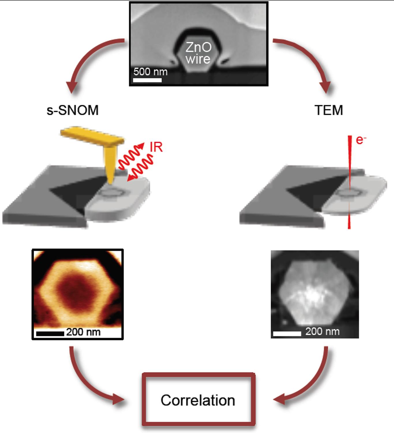
The joint Basque research team has developed a new method named correlative infrared-electron nanoscopy for taking s-SNOM – a relatively new technique that allows for nanoscale infrared imaging and spectroscopy – and TEM images of one and the same nanostructure. “We have developed a special sample preparation that allows combining these two techniques using a unique sample”, explains Andrey Chuvilin, the nanoGUNE’s TEM expert. “Thanks to our method we can better understand the properties of materials at the nanometer scale and this opens new avenues for studying widely different material properties and their mutual relationship”, says nanoGUNE’s researcher Johannes Stiegler.
This work is in line with cutting edge research in modern materials science and especially in nanotechnology, where the understanding of the properties of materials at the nanometer scale is an ultimate goal. A variety of high-resolution imaging techniques providing different information about the different material properties exist. It is, however, the combined use of the different characterization techniques that will further the understanding of functional nano materials.
Correlative infrared-electron nanoscopy is a good example of combining different imaging methods. While TEM is a well established imaging technique in materials science, providing structural information with atomic resolution, s-SNOM is a imaging method yielding maps of the chemical composition and conductivity with a spatial resolution of less than 20 nm. “As we demonstrate in our study, the correlation of the TEM and SNOM images will help to obtain a deeper and more comprehensive understanding of the material properties at the nanometer level”, Stiegler states.
THE POTENTIAL
In order to demonstrate the potential of correlative infrared-electron nanoscopy the researchers have studied cross-sections of ZnO nanowires using a NeaSNOM from Neaspec GmbH (www.neaspec.com) and the Titan TEM from FEI Company (www.fei.com). These nanowires are of high technological relevance due to their potential to be used as universal electron transport building blocks in different technological applications such as solar cells, light emitting sensors and piezoelectric nanogenerators. Although being of great importance, very little is known about the local conductivity within these wires.
From the infrared s-SNOM images the researchers find a radial conductivity profile, whose origin cannot be explained without further information. The origin of this profile, however, can be explained by studying the local structural properties with TEM, where in the regions of low conductivity the ZnO wire exhibit significant crystal defects. From the two different images an inverse correlation between defect density and free-carrier (conductivity) concentration can be concluded.Ramón Tena-Zaera, Head of Photovoltaics Unit at IK4-CIDETEC, explains that the novel technique “allows us, for the first time, to obtain all this information about one unique sample”. “Our results open new avenues in the growth and device integration of ZnO nanowires. Until now, for example, the scientific community has focused on obtaining nanowires with diameters as thin as possible because it was considered they had more potentiality. However, our results suggest that lateral growth – a bigger diameter – is advantageous to obtain defect-free and high electronic conductivity materials”, says Tena-Zaera.
Although shown for a special sample, “the method of correlated infrared-electron nanoscopy has a much broader applicability – concludes Rainer Hillenbrand, Nanooptics Group Leader at nanoGUNE and coordinator of the study – and has great potential to study novel materials such as graphene, topological insulators, phase change materials, or biological and organic nanostructures”.
Published manuscript:
Stiegler J.M., Tena-Zaera R., Idigoras O., Chuvilin A. and Hillenbrand R. Correlative infrared–electron nanoscopy reveals the local structure–conductivity relationship in zinc oxide nanowires. Nat. Commun. 3:1131 doi: 10.1038/ncomms2118 (2012).