Coexistence of superconductivity and charge density waves observed
Scientists at Max Planck Institute for Solid State Research, BESSY II Synchrotron and nanoGUNE have discovered that an artificial structure composed of alternating layers of ferromagnetic and superconducting materials induce Charge Density Waves deeply into the superconducting regions, indicating new ways to manipulate superconductivity. The results have been published in Nature Materials.
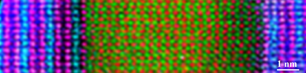
Scanning electron microscopy in combination with EELS electron spectroscopy permits to visualize atomic positions of the individual atoms in the heterostructure: Superconducting regions of YBaCuO are identified by yttrium (blue) and copper (pink), the ferromagnetic layers by manganese (green) and lanthanum (red). Courtesy MPI Stuttgart.
High-Tc superconductors were discovered 30 years ago: A class of ceramic metal oxide materials was found to pass electrical current without energy losses. In contrast to conventional superconductors that have to be cooled almost to absolute zero, this property appears already at comparably high temperatures. In prototypical yttrium barium copper oxide (YBaCuO), the transition temperature is 92 Kelvin (minus 181 degrees centigrade). Hence, liquid nitrogen suffices as coolant to reach the superconducting phase. The discovery of high-temperature superconductivity has started a quest for applications, which are being implemented now. Until now, however, the microscopic mechanism of high-Tc superconductivity is still matter of debate.
Superconducting and ferromagnetic thin layers
A team of scientists involving Prof. Bernhard Keimer, MPI for Solid State Research, Dr. Eugen Weschke, HZB and Dr. Santiago Blanco-Canosa (IKERBASQUE Research Fellow at nanoGUNE) have now investigated an artificial layer system composed of alternating ferromagnetic material (La1-xCaxMnO3) and nanolayers of YBaCuO with thicknesses between 10 nm and 50 nm. As interfaces often determine the properties of such heterostructures, physicists were particularly interested in their role for the present system. During Fraño´s PhD work using resonant x-ray diffraction at BESSY II, researchers could detect tiny collective modulations of valence electrons around Cu atoms in the YBaCuO layer. Data analysis revealed that the resulting charge density wave does not remain located close to the interface but extends across the whole layer. “This finding is quite a surprise, as previous studies revealed a strong tendency of superconductivity to suppress the formation of charge density waves”, explains Frano.
Charge density wave is stabilized
“Dynamic Charge Density Waves in YBaCuO were observed to strongly compete with superconductivity. Engineering artificial superlattices of ferromagnetic and superconducting materials allowed to stabilize charge density waves: YBaCuO remains superconducting while the charges arrange in a periodic structure”, explains Blanco-Canosa, The results pave the way to the stabilization of collective phenomena in materials that will allow scientists to control and manipulate their physical properties on demand.
Long-range charge-density-wave proximity effect at cuprate/manganate interfaces, A. Frano, S. Blanco-Canosa, E. Schierle, Y. Lu, M. Wu, M. Bluschke, M. Minola, G. Christiani, H. U. Habermeier, G. Logvenov, Y. Wang, P. A. van Aken, E. Benckiser, E. Weschke, M. Le Tacon & B. Keimer, Nature Materials (2016) doi: 10.1038/nmat4682