dd
CIC nanoGUNE
  • en
  • es
  • eu

User account menu

  • Log in

Main Menu ES

  • nanoGUNE
    • At a Glance
    • Organization & Funding
    • People
    • Join us
    • Life
    • Newsroom
    • nanoPeople
  • Research
    • Research
    • Publications
    • Projects
    • External services
  • TechTransfer
    • TechTransfer
    • Start-ups
    • IP Portfolio
    • Industry collaborative research positions
    • Strategic lines
    • External services
    • News & events
  • Training
    • Master projects
    • Bachelor Final Projects
    • Summer Internships
    • Education University PHD
  • Society

User menu

  • Log in
  1. Home
  2. Review on diffusion phenomena in ALD, highlighted by Semiconductor Science and Technology

Review on diffusion phenomena in ALD, highlighted by Semiconductor Science and Technology

14/03/2013

Semiconductor Science and Technology has selected Mato Knez’s review on Diffusion phenomena in Atomic Layer Deposition (ALD) as a highlight of 2012. The magazine’s annual selection by the Editorial Board “represents the breadth and excellence of the work published in 2012. All articles were selected for their presentation of outstanding research, popularity with their online readership and high praise from referees”.


As it is mentioned in the review “Atomic layer deposition is a mature technology for the deposition of conformal thin films. During the ALD process or in a post-treatment, a variety of diffusion phenomena can occur which can not only deteriorate the desired product, but also can be used to fabricate materials or structures in a novel way. This special issue reviews some of the observed diffusion processes and strategies to make use of those.”

The review can be read here.


Original publication Mato Knez 2012 Semicond. Sci. Technol. 27 074001 [doi:10.1088/0268-1242/27/7/074001]


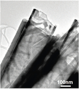
Typical TEM image of Al2O3/ZnO/Al2O3 microtubes (~18/10/44 nm) annealed at 700 °C for 12 h. Broken tubes clearly reveal physical separation and delineation between the inner and outer spinel tubes. The image confirms increased roughness of the spinel layers along the length of the tube, on the surfaces adjacent to the Kirkendall voids. Image adapted with permission. Copyright 2009 by the American Chemical Society.

Tags
ALD
  • whatsapp
  • facebook
  • twitter
  • linkedin
  • print

Related news

  • 06/05/2025

    NanoGUNE starts building the Quantum Tower

  • 01/04/2025

    Donostia, the spintronics and orbitronics capital

  • 31/03/2025

    Mariana Medina, interviewed on Radio Euskadi about “How to create microbots to help conceive a baby”

  • 14/02/2025

    Review Article Highlights 25 Years of Modern Near-field Optical Nanoimaging

  • 11/02/2025

    Scientists synthesize 2D polyaniline crystal with unique metallic out-of-plane conductivity

  • CIC nanoGUNE
  • Tolosa Hiribidea, 76
  • E-20018 Donostia / San Sebastian
  • +34 943 574 000 · nano@nanogune.eu
  • Facebook Twitter Youtube Linkedin Instagram Subscribe to our Newsletter

Menú pie principal

  • nanoGUNE
  • Research
  • TechTransfer
  • Training
  • Society
  • nanoPeople

Menú pie servicios

  • External services
  • Publications
  • Seminars
  • Join us
  • Newsroom
  • Contractor profile
  • Corporate Compliance

Menú pie grupos

  • Nanomagnetism
  • Nanooptics
  • Self Assembly
  • Nanobiosystems
  • Nanodevices
  • Electron Microscopy

Menú pie grupos 2

  • Theory
  • Nanomaterials
  • Quantum-Probe Microscopy
  • Nanoengineering
  • Quantum Hardware

Funded by

  • EJ/GV
  • Diputación
  • FEDER
  • FEDER
  • Ministerio de Ciencia e Innovación

Member of

  • BRTA
  • SOMM

Distinctions

  • Distinción de Excelencia María de Maeztu 2022-2025
  • Excellence Research
  • UNE-166002

Menú legales

  • Accesibility
  • Legal notice
  • Privacy policy
  • Cookies policy
  • Confidentiality policy
by ACC