Electrons trapped in a defect
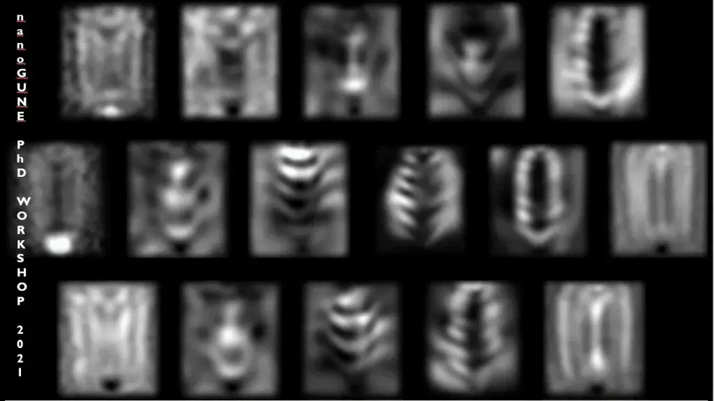
The most intriguing things we observe are the ones we don’t understand. Especially when the length and energy scales are beyond our everyday experience and the concepts reach the very edge of abstraction. In this series of 82x70 nm Scanning Tunneling Microscopy maps we see the density of electrons at different energies trapped in a distorted portion of a graphene layer.On the right and left sides of the panel, we see the two starting points of the lattice distortion, among them a vertical wave pattern extends towards the sides. In the central figures the wavefunction develops in more variegated manners.The system is challenging to simulate without knowing the exact atomic structure. And is an explicit portrait of the quantum mechanical nature of the electrons.
Image taken by Stefano Trivini.