Engineering electron pathways in 2D-topological insulators
In a recent article published in Physical Review Letters researchers from CIC nanoGUNE, the Rudolf Peierls Centre for Theoretical Physics of Oxford, together with colleagues from Wuerzburg and Stanford University reported new insight into the electronic conduction and interference on 2D-topological insulators - an exotic kind of insulators that conduct only at the edge and that could be key for the development of a new generation of electronic devices.
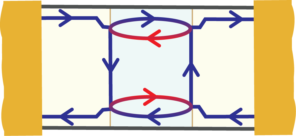 Schematic representation of the electronic behavior in the device described in the article. The arrows represent quantum channels where electrons propagate. Eectrons are allowed to change direction only at the central area, resulting under certain conditions in constructive interference.
For decades, insulating materials were thought to be “boring” materials from an electronics point of view, since electrons are immobile and cannot contribute to electrical conduction. Recently, a different class of insulators was proposed and experimentally found. We call them “topological insulators”, as their electronic structure can be mathematically classified to be different than the usual, boring, “trivial” insulators.
A fascinating property of topological insulators is that while remaining insulating in the bulk, they are very good conductors at the edge. At those edges, electrons travel in quantum channels in either direction, like in a two- lane highway. Also like on a highway, U-turns are forbidden: electrons on the edge cannot change direction without breaking the rules. The application of an external magnetic field lifts this prohibition and allows electrons to turn.
The recently published research, lead by Reyes Calvo, Ikerbasque Fellow at CIC nanoGUNE, and Fernando de Juan, currently at Rudolf Peierls Centre for Theoretical Physics, Oxford and joining the Donostia International Phisics Centre (DIPC) as Ikerbasque Fellow in 2018, reports the interplay of quantum edge states across a lateral junction in a HgTe quantum well, a canonical 2D topological insulator. From their results, they extract new information on the fundamental properties of topological edge states and propose strategies to fine-tune their interaction.
"In our work, we test the consequences that allowing electrons to turn have in the conduction of our devices. We also show how under certain circumstances, electrons allowed to return seem to do it in an orderly manner, as if in some kind of round-about, generating a constructive interference.", Calvo explains.
This work contributes new insight into the fundamental properties of the edge states and their conduction properties in 2D-topological insulators. This kind of proposals to control the properties and interactions of these states are key for their application in the development of a new generation of electronic devices based on quantum fundamental properties of materials.
Interplay of Chiral and Helical States in a Quantum Spin Hall Insulator Lateral Junction
M. R. Calvo, F. de Juan, R. Ilan, E. J. Fox, A. J. Bestwick, M. Mühlbauer, J. Wang, C. Ames, P. Leubner, C. Brüne, S. C. Zhang, H. Buhmann, L. W. Molenkamp, and D. Goldhaber-Gordon