Nature Materials: High Resolution TEM reveals chemical bonds
The combination of HRTEM experiments and first-principles electronic structure calculations opens a new way to investigate electronic configurations of point defects, other non-periodic arrangements or nanoscale objects that cannot be studied by an electron or X-ray diffraction analysis. In the article published in Nature Materials (Nature Mat. 10, 209-215, cover page, and News&Views article by K. U. Urban), the authors show experimental evidence of charge redistribution due to chemical bonding by means of high-resolution transmission electron microscopy (HRTEM) in two different systems: nitrogen-substitution point defects in graphene, and single-layer hexagonal boron nitride.
The redistribution of charge that occurs when free atoms are arranged into a solid or molecule is of tremendous interest. It is the distribution of the binding electrons and their energy levels that defines, to a large extent, the properties of a material However, the redistribution of charge due to chemical bonding is small compared with the total charge density, and therefore difficult to measure. The effect of binding electrons on HRTEM image contrast has been explored through calculations in previous studies, but the effects were not detected experimentally. The article shows how charge transfer between neighbouring atoms can be analyzed on the basis of atomically resolved HRTEM.
As a first example, the electronic configuration around nitrogen-substitution is analyzed. In this case, the authors demonstrate that the electronic configuration on the carbon atom next to the nitrogen is perturbed by the defect. In other words, electron scattering on the carbon atom next to the nitrogen is significantly different from electron scattering on a carbon atom elsewhere in the graphene sheet. In the second example, the ionic character of single layer hexagonal boron nitride (hBN) is confirmed from HRTEM measurements. Both examples are impossible to analyze using standard diffraction techniques, which are limited to sufficiently large periodic structures not available in the case of point defects or single-layer structures.
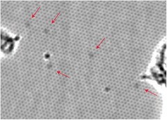
TEM image HRTEM Image showing five nitrogen substitution defects in graphene marked by red arrows.
The method uses density-functional theory (DFT) to calculate the expected electron density that can be used to predict the atomic scattering potential for the electrons. By solving the Schrödinger equation for this potential, a local atomic-scale phase modulation can be calculated for the electron wave, which will be observed as contrast in an state-of-the-art aberration corrected transmission electron microscope, providing the evidence of the charge transfer related with the binding electrons.
The method described in the article opens new frontiers for electron microscopy techniques and shows the interest of going beyond the so called “independent atom model”, which neglected the effects of the binding electrons, in order to see, measure, and understand the way atoms integrate into solids and molecules.

Transmission electron microscopy has reached unprecedented resolution and can provide structural information down to the single atomic level. It is now shown that a properly designed experimental analysis also allows the charge distribution around a single atomic dopant to be monitored, demonstrating the possibility of TEM to provide electronic as well as structural information. (From Nature Materials).