Business news

The new enterprise, due to be set up in December, will be optimising cell cultures by combining Raman spectroscopy, nanoparticles and AI. This technology allows the early detection of culture anomalies and greater efficiency in accelerating cancer treatments such as CAR-T.
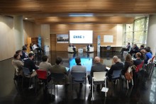
Today, nanoGUNE welcomed the Hamaiketako de Gerentes (CEO's Breakfast) organized by ENNE Fundazioa, bringing together 35 CEOs from Basque companies to reflect on the role of leadership face to technological challenges.
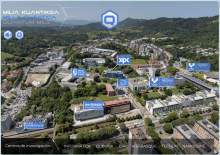
Starting today, Donostia has a scientific-technological route that can be explored on foot or virtually. This outreach initiative, promoted by the Basque Government and involving CIC nanoGUNE along with six other centers, highlights and recognizes the Basque scientific leadership in quantum science and technologies.
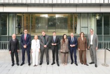
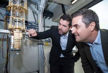
The inauguration of IBM's quantum computer in Donostia marks a significant milestone in the advancement of quantum technology in the region. The event, presided over by Lehendakari Imanol Pradales, was attended by prominent figures from the scientific and technological fields, including nanoGUNE's Director General, Jose M. Pitarke, and Ainara Garcia Gallastegui, Director of Technology Transfer, who participated in the round table titled “Building the Global Quantum Ecosystem.”
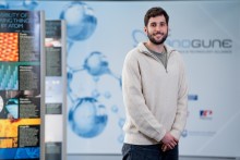
A business initiative led by postdoctoral researcher Dr. Javier Plou, from the Nanoengineering Group, has been selected among the top 10 start-ups in the Health category of the prestigious EIT Jumpstarter program. The project, which focuses on developing novel spectroscopic technologies for monitoring advanced CAR-T therapies, was first prioritized by Basque Tek Ventures, validating its potential for real-world impact.

MindSens wins the III Global Graphene Call with a breakthrough dementia diagnostic device: a portable, accurate, and affordable home-use diagnostic tool that could bring early dementia detection into homes and clinics around the world. The international call launched by CIC nanoGUNE, BerriUp, Graphenea, Fomento de San Sebastián, and BIC Gipuzkoa, seeks revolutionary ideas that tackles the potential of graphene in industrial and technological applications.
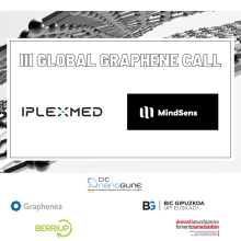
The international call launched by CIC nanoGUNE, BerriUp, Graphenea, Fomento San Sebastián and BIC Gipuzkoa, seeks revolutionary ideas that tackles the potential of graphene in industrial and technological applications. The two winning companies will benefit from a tailored four-month training and acceleration program, with access to resources provided by the organizing entities.
Quantum Motion will establish in Euskadi through an agreement with CIC nanoGUNE. The goal will be scientific-industrial collaboration to design the first silicon quantum chip.
Through a joint effort, CIC nanoGUNE, BerriUp, Graphenea, Fomento de San Sebastián and BIC Gipuzkoa are seeking revolutionary ideas that harness the potential of graphene in industrial and technological applications. Entrepreneurs and companies wishing to take part must present their own original projects from 13 September to 13 October 2024. The organizing entities offer a unique set of resources to support the selected projects.

The Basque nanoscience research center opens a new group for the development of quantum hardware.
A new tower will be built, which will be housing the laboratories of the new group and also a leading scale-up company in quantum technologies.
NanoGUNE will be developing in San Sebastian chips for the construction of quantum computers based on semiconductor technology.