2D Spintronics
 Overview
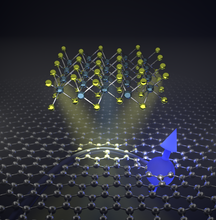
2D materials have raised a lot of interest since graphene, a monolayer of carbon atoms with extraordinary properties, was isolated in 2004 using the scotch tape technique [1]. Since that, a plethora of 2D materials with extraordinary properties which range from unprecedentedly large carrier mobilities to record light absorption efficiencies are currently being characterized. Moreover, their layered nature enables the creation of new metamaterials in which different 2D materials are stacked on top of each other. These metamaterials are called van der Waals heterostructures [2].
In the 2D spintronics research line, we study the creation, transport and manipulaton of spin currents in van der Waals heterostructures which are based on graphene and other 2D materials such as transition metal dichalcogenides (TMDs) or hexagonal boron nitride (hBN). While graphene has the longest spin relaxation length at room temperature and allows for efficient spin transport, TMDs are a source of spin-orbit coupling that, when imprinted on the graphene by proximity, modifies the properties in graphene allowing for spin manipulation. We also introduce the 2D insulator hBN in our graphene-based spintronic devices to improve graphene’s properties [3] and as a gate dielectric to control the carrier density.
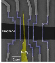
Following this approach, we perform experiments on electric-field control of spin transport [4] and proximity-induced spin-to-charge conversion in heterostructures of graphene and TMD [5]. Because efficient ways to convert charge currents into spin currents and vice-versa are crucial for spintronic applications, we also study spin-to-charge conversion in bulk metals in combination with graphene [6] to identify the most optimal systems and conditions.
Currently, we are also extending our studies into more exotic material systems such as graphene in combination with topological insulators, oxides, semimetals, and organic materials. For more details of the research lines using these materials, refer also to the molecular devices and metal spintronics sections.
References
[1] K. S. Novoselov, A. K. Geim, S. V. Morozov, D. Jiang, Y. Zhang, V. Dubonos, I. V. Grigorieva and A. A. Firsov, Science 306, 666 (2004).
[2] A. K. Geim and I. V. Grigorieva, Nature 499, 419 (2013).
[3] J. Ingla-Aynés, R. J. Meijerink and B. J. van Wees, Nano Letters 16, 4825 (2016).
[4] W. Yan, O. Txoperena, R. Llopis, H. Dery, L. E. Heuso and F. Casanova, Nature Communications 7, 13372 (2016).
[5] C. K. Safeer, J. Ingla-Aynés, F. Herling, J. H. Garcia, M. Vila, N. Ontoso, M. R. Calvo, S. Roche, L. E. Hueso and F. Casanova, Nano Letters 19, 1074 (2019).
[6] W. Yan, E. Sagasta, M. Ribeiro, Y. Niimi, L. E. Hueso and F. Casanova, Nature Communications 8, 661 (2017).