Nanofabrication
Overview
Our expertise includes methods as diverse as electron beam lithography (EBL) or focused electron and ion beam induced deposition (FEBID/FIBID). We can engineer improved materials with high degree of control to explore the extreme possibilities of our techniques. The extensive knowledge acquired enables us to build final devices with high performances.
In particular, EBL is a powerful technique that can be used to design nanodevices with a resolution down to a few nanometers. On the other hand, FEBID or FIBID can be used to grow materials with fine tuning or to facilitate the interconnexion with other structures of the nanodevices. In addition, these two techniques are employed in the preparation of heterogenous structures or to modify the surface of 2D materials such as graphene or hexagonal boron nitride (hBN). Our work goes through the combination of different materials and geometries and the consequent study of the capabilities of the devices.
Examples
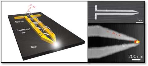
1) Infrared light waveguides, made of two metal wires. It is a concept adapted from the idea of transmission lines. We manage to nanofocus infrared light to a 60 nm spot size by reducing the width of the cable. These devices have applications in areas such as nanoscale imaging, sensing, nanoscale optical circuitry, etc. They were fabricated with EBL and metal lift-off on a silicon substrate and consist in 40 nm of gold thermally evaporated in high vacuum [1].
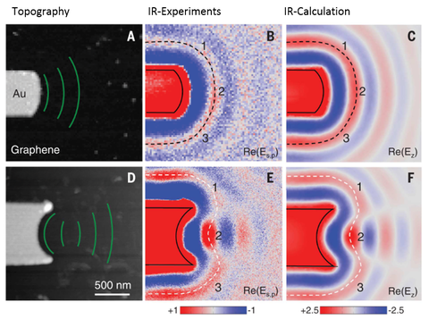
2) Graphene plasmon focusing by tailoring the antenna geometry: a concave antenna extremity was fabricated to focus graphene plasmons. The shape of the antenna determines the wavefronts that are launched. In this case, the antennas were fabricated on (100)-oriented CaF2, with EBL and metal lift-off. A 5-nm-thick SiO2 layer was previously sputtered on the substrate, and CVD graphene transfered onto it [2].
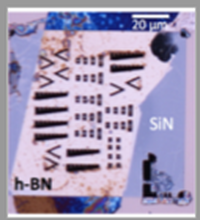
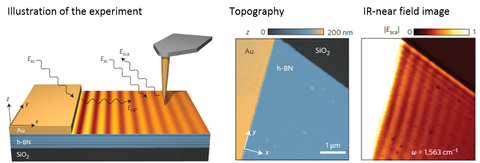
3) Infrarred phonon polaritons in a thin hBN waveguide exhibit hyperbolic dispersion and subwavelength-scale field confinments. Samples were fabricated by mechanical exfoliation of hBN on blue Nitto tape and transfered onto the Si/SiO2 chip. The gold edge was then designed with EBL and deposited by electron-beam evaporation in ultrahigh vacuum [3].
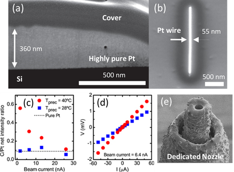
4) Pt structures performed by FEBID [4]. The depositions (a, b) were performed by simultaneous supply of O2 and organic precursor with a dedicated concentric nozzle (e). By adjusting the flux-ratio between the O2 and the precursor, highly pure Pt structures can be obtained (measured as C/Pt). Since deposition and purification take place in the same step, it is possible to obtain highly homogeneous and void-free structures with the desired thickness. Furthermore, by decreasing the precursor temperature and the beam currents, structures with a good definition and high purity can be obtained (c). Resistivities of 89±10 and 60±5 μΩ cm are obtained using precursor temperatures of 40 and 28 °C, only 6 times higher than pure bulk Pt (10.6 μΩ cm) (d).
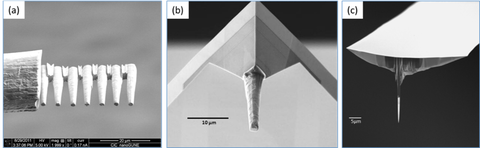
5) Resonant antenna probes performed by FIBID [5]. The tip apex of a standard Si atomic force microscopy (AFM) cantilevers were cut. Then a several micrometer long rod was milled out of a 25-μm-thick Au wire (panel a) and attached to the cut Si tip by FIBID of SiOx (panel b). The Au rod was shaped by the ion beam until a sharp high aspect ratio cone was formed (panel c). By adjusting the milling parameters, the conical angle of the tip can be varied. The radius of curvature of the tip apex can be as small as 10 nm.
References
[1] M. Schnell, P. Alonso-González, L. Arzubiaga, F. Casanova, L. E. Hueso, A. Chuvilin, and R. Hillenbrand, Nature Photonics 5, 283 (2011).
[2] P. Alonso-González, A. Y. Nikitin, F. Golmar, A. Centeno, A. Pesquera, S. Vélez, J. Chen, G. Navickaite, F. Koppens, A. Zurutuza, F. Casanova, L. E. Hueso, and R. Hillenbrand, Science 344, 1369 (2014).
[3] E. Yoxall, M. Schnell, A. Y. Nikitin, O. Txoperena, A. Woessner, M. B. Lundeberg, F. Casanova, L. E. Hueso, F. H. L. Koppens and R. Hillenbrand, Nature Photonics 9, 674 (2015).
[4] E. Villamor, F. Casanova, P. H. F. Trompenaars, and J. J. L. Mulders, Nanotechnology 26, 095303 (2015).
[5] F. Huth, A. Chuvilin, M. Schnell, I. Amenabar, R. Krutokhvostov, S. Lopatin, and R. Hillenbrand, Nano Letters 13, 1065 (2013).