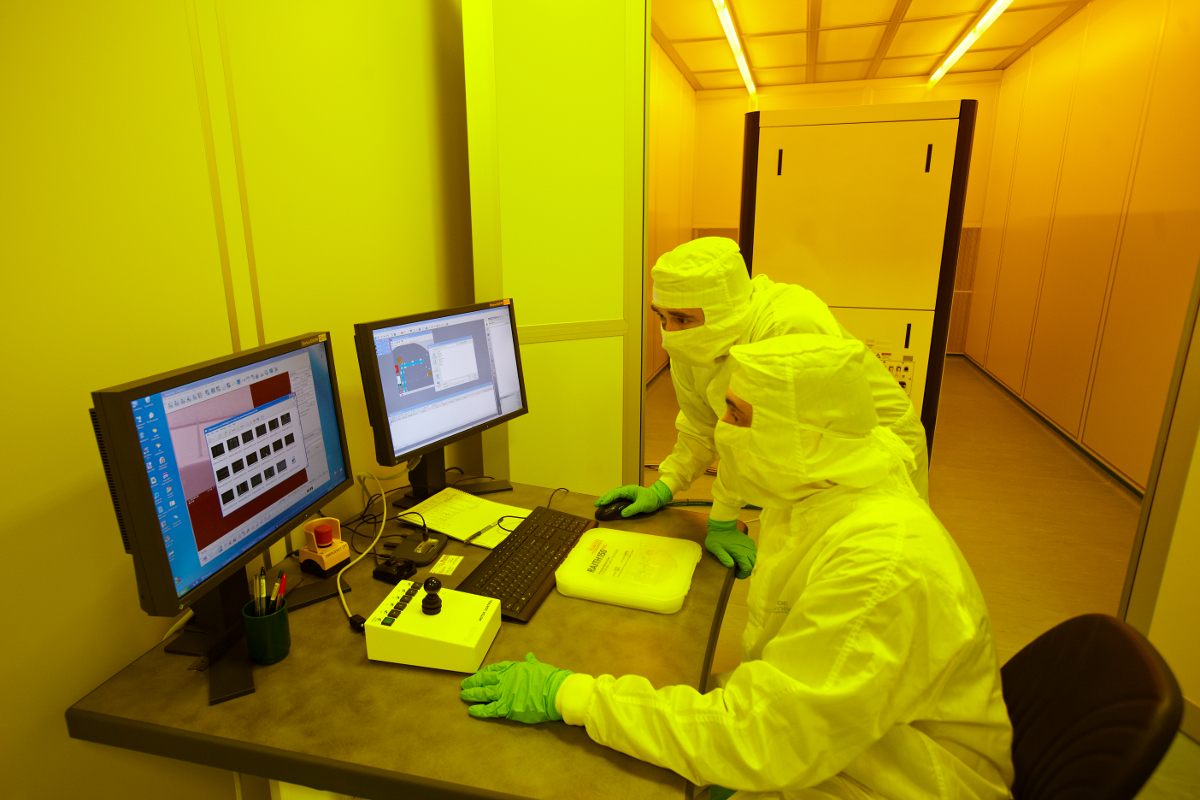
Electron-Beam Lithography (Raith -150-TWO / E-line)
Offered as External Service
E-Beam Lithography used for design and nanostructure fabrication.
Research group
Technical characteristics
Electron beam column and optics:
- Electron source: Schottky field emitter ZrO/W.
- Beam energy range: 100 V to 30 kV in 10 V steps.
- Beam current range: 5 pA – 20 nA.
- Beam size (Gaussian beam):
- 2 nm at 20 kV at 3 mm working distance.
- nm at 1 kV at 3 mm working distance.
- Deflection system with writing field size range: from 0.5 µm up to 2 mm
- Laser interferometer controlled stage (res. 2 nm, repeatability <<50 nm)
- Aperture: 7 to 120 μm
- 20 MHz high speed pattern generation
- Automated height sensing
- Minimum feature size ≤ 20 nm.
- Possibility to pattern areas of up to 4” wafers
Cleanroom
CR1 - eBeam Lithography Room
Related Techniques
Cleanroom
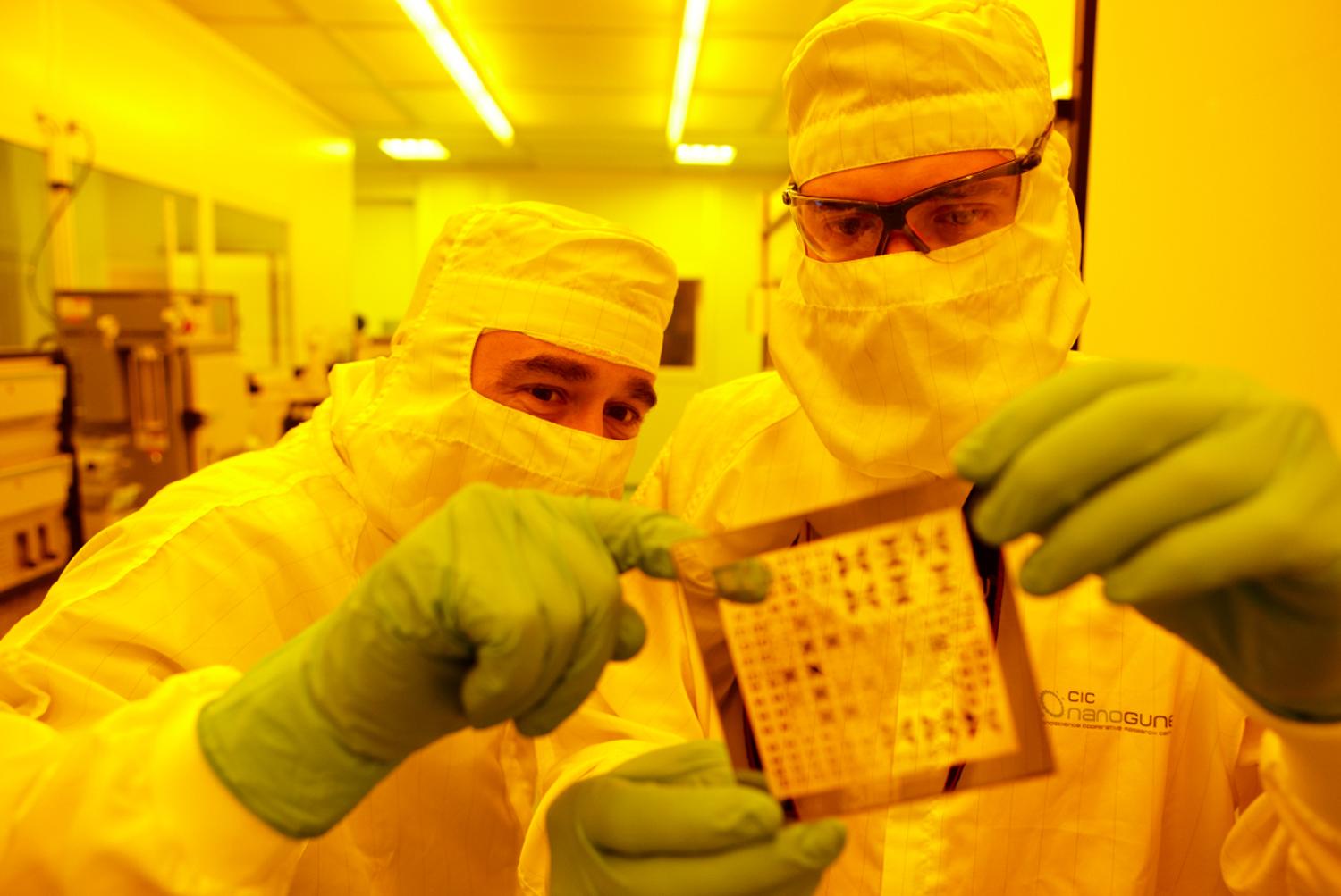
The nanoGUNE cleanroom, dedicated to fabricate and characterize the properties of materials on the nanoscale, ia a 300m2 laboratory where the air purity is under strict supervision.
Equipment
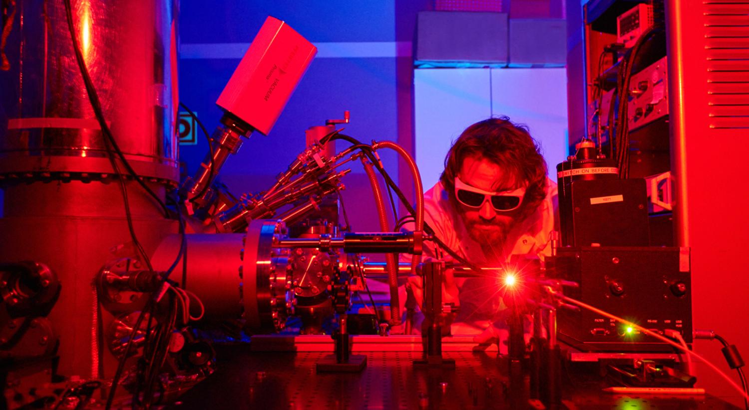
State-of-the-art equipment, including electron and scanning-tunneling microscopes, as well as other nanofabrication and characterization tools, are managed by specialists and used by researchers from a wide variety of fields.