Related news by tag Nanodevices
The Nanodevices group participates in the 2D-INK Fet Open project

The Nanodevices group at nanoGUNE is one of the 9 partners of the project. Its contribution will be to fabricate and test transistors with the semiconductor ink provided by other partners in the consortium. NanoGUNE will also take care of the miniaturization of the devices, having in mind possible electronic applications, such as wearables. With this purpose, they will receive 297,600€ for a 3 years period.
The company Graphenea, launched by nanoGUNE and a group of private investors in 2010, will also participate in the project. The collaborative research-team is completed by six more European university partners: Algoritmi Center of the Universidade do Minho (Braga, Portugal); ICMol Institute of the Universitat de Valencia (Valencia, Spain); the Technische Universität München (Munich, Germany); the Katholieke Universiteit Leuven (Leuven, Belgium); the Universität Wien (Vienna, Austria); and the University of Nottingham (United Kingdom).
The FET-OPEN (Future and Emerging Technologies) projects of the European Union support research lines in early stages, based on ideas that may arise new technology lines. Thus, the EU initiative encourages scientists and engineers from many disciplines to cooperate in research projects that promote scientific progress. It is noteworthy, too, that the European program FET -OPEN is a highly competitive call: only 24 of the 643 submitted projects (3.7%) have been funded across Europe.
Patents
The development of semiconductor inks from two-dimensional materials with different properties represent, according to the coordinator of the project, Aurelio Mateo-Alonso, "a major breakthrough in the field of new materials for the next generation of ultra-thin electronic devices such as transistors, LEDs, solar cells, protodetectors, etc.". The researchers also predicts the submission of patents, given the technological possibilities of 2D-INK and the involvement of a private company.
CIC nanoGUNE and INTEL bring the MESO technology a step closer to reality
Finding a replacement to current CMOS technology in electronics that can be smaller, faster and, most importantly, with less energy consumption is a global challenge. Recently, Intel proposed what they refer as the “MESO” logic, a new technology that combines memory, interconnections and logic requirements for future computing needs, which might allow to maintain Moore’s law beyond CMOS while being more energy efficient.
In order to prove the feasibility of this disruptive technology, Intel and nanoGUNE have been joining forces in the last one and a half years. “The core element of MESO logic has two active parts. One part “reads” the information from the memory (a magnetic bit), which uses a unique effect known as ‘spin Hall effect'. The other one “writes” the magnetic bit using the magnetoelectric effect of certain materials”, explains Ikerbasque researcher Fèlix Casanova, who is leading the “MESO” project at nanoGUNE. Whereas the team of Components Research at Intel have proposed this technology, the group of nanodevices at nanoGUNE is a world-renown expert in the spin Hall effect. “According to the calculations of Intel’s team, we need the two parts to operate at the same voltage for the circuit to work: 0.1 Volt. The biggest problem is that previous devices using this spin Hall effect could only provide 10 nanoVolt, that is, 10 million times less. The big challenge is thus to increase this output voltage for the “reading” part”, adds Casanova.
Now, the first results of these joint efforts are being published in the journal Nature Electronics. The groups of nanoGUNE and Intel have been able to increase by 10,000 times this voltage, by simply using a better design but with the standard material for this effect, platinum. Although they still did not reach the final value for this technology to work, they unveil different paths on how to achieve it. First, the signal given by the device they have designed scales when the dimensions are reduced, which is a requirement for any technology to be introduced in the market (otherwise miniaturization would not be possible). Second, they identify the exact role of the materials in the device, and estimate that certain materials (like the recently discovered topological insulators) have the necessary properties that should allow them to bridge the remaining gap of 1,000 times enhancement for the 0.1 Volt goal. These results, thus, bring the MESO technology a step closer to reality.
Electrical control of magnetism by electric field and current-induced torques
Albert Fert, French physicist and winner of the Nobel Prize in Physics in 2007, is one of the discoverers of giant magnetoresistance, a physical effect that revolutionised hard disk technology, allowing a huge increase in its capacity. His research enabled the capacity and applications of the hard disk drive to be increased, and he is now working towards a new generation of microprocessors t
Tracking slow nanolight in natural hyperbolic metamaterial slabs
Hyperbolic materials are very special because they behave like a metal in one direction, but like an insulator in the other. Until now, these materials have been used to fabricate complex nanostructures that permit subwavelength-scale imaging, as well as the focusing and controlling of light at the nanoscale. However, in order to fully exploit their potential, it is necessary to study and understand how light behaves inside them.
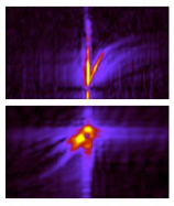
The work lays the foundations for studying the precise manner in which light travels through complex optical systems at the subwavelength scale in extremely high levels of detail. Such a capability will be vital for verifying that future nanophotonic devices, perhaps with biosensing or optical computing applications, are functioning as expected.
"The difficulty in performing the reported experiments is the extremely short wavelength of light when it is inside a hyperbolic material” explains Ikerbasque Professor Rainer Hillenbrand, leader of the nanooptics group at nanoGUNE. When light moves inside the material – in our case mid-infrared light in a 135 nm boron nitride slab - it travels in the form of what we call a polariton, where the light is actually coupled to the vibrations of the matter itself".
These polaritons can be considered a double-edged sword to the scientists trying to study them. On the one hand, they squeeze light into much smaller volumes than is normally possible. This is helpful for a wide range of applications that require the manipulation of light in tiny spaces, such as detecting and identifying individual molecules. On the other hand, this ultra-high confinement means that special techniques have to be developed to look at their behavior.
Edward Yoxall, who performed the experiments at nanoGUNE along with Martin Schnell, elaborates: "Because the wavelength of a polariton is so small, we cannot use 'conventional' optical equipment, such as lenses and cameras, to image it. Instead, we have to use a special type of microscope." This microscope - a scattering-type scanning near-field infrared microscope - is capable of seeing details 1000 times smaller than a standard infrared microscope, visualizing "objects" of just 10 nanometers.
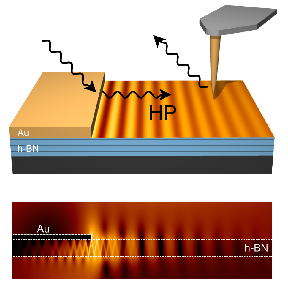
"But it's not just the spatial resolution that makes tracking polaritons tricky", continues Yoxall. "If we want to see how a polariton moves, we need to detect and track it in both space and time. This can be accomplished by using extremely short flashes of light - or pulses- that are just 100 femtoseconds long." That is an extremely small number; less than one millionth of a millionth of a second. By using these very short flashes in combination with their near-field microscope, the researchers are able to watch the polaritons passing different locations along the boron nitride slab, allowing for measuring their speed.
By using both the space and time information that is gathered during the experiment, the scientists have been able to exactly determine how the polariton was travelling. The time- and space-resolved maps revealed a range of intriguing behaviors of the polaritons, including a dramatic slowing down of the pulse velocity - below 1 percent of the light velocity in vacuum- and a reversal of the direction in which the polariton waves were propagating in relation to the direction of the energy flow.
“An exciting result is the speed at which the polariton moves”, says Yoxall. “There’s a lot of interest in slow light, and what we’ve shown here is a novel way of achieving this.” Slow light in conventional photonic structures has great potential for manifold applications in sensing and communication technologies, owing to enhance light-matter interactions. The deep subwavelength-scale confinement of slow polaritons in hyperbolic materials could help to miniaturize these devices.
A project coordinated by CIC nanoGUNE receives nearly 4 million euros from the European Commission
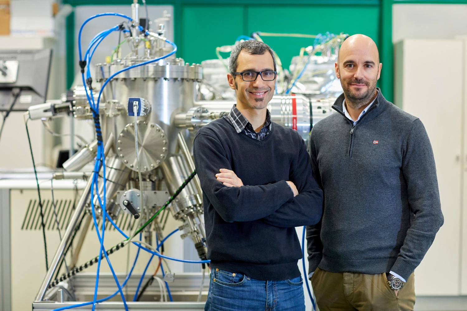
SPEAR has been selected by the European Commission for funding within its ITN programme. The 4-year project will receive nearly 4 million euros. This funding will be used mainly to fund the recruitment and high-level training of 15 pre-doctoral researchers. SPEAR is led by Fèlix Casanova, an Ikerbasque Research Professor in the Nanodevices Group at nanoGUNE.
“The research aims to find new materials with strong spin-orbit coupling, to explore new phenomena associated with these materials, and to develop devices based on these phenomena for the upcoming generation of computer memories and processors,” said the head of the project at nanoGUNE. “Unlike conventional RAM memory, data will not be stored in the form of electric charge or current flows, but by means of magnetic storage components in the next generation of memories, such as MRAM (Magnetic Random Access Memory). To substitute current microprocessors using silicon transistors we also have various candidate technologies, such as spin logic or MESO logic, machine learning and neuromorphic computing, which would stand to benefit from these new materials,” added Fèlix Casanova.
Transforming Digital Technologies through the SPEAR ITN project
The overarching scientific and technological objective of this research program is to study materials with strong spin-orbit coupling, novel phenomena in these materials, and to build devices based on these phenomena for the next generation of memories, such as magnetic random-access memory (MRAM), and beyond-CMOS technology, e.g., spin-orbit-based logic, machine learning or neuromorphic computing.
On-chip observation of THz graphene plasmons
Radiation in the terahertz (THz) frequency range is attracting large interest because of its manifold application potential for non-destructive imaging, next-generation wireless communication or sensing. But still, the generating, detecting and controlling of THz radiation faces numerous technological challenges. Particularly, the relatively long wavelengths (from 30 to 300 μm) of THz radiation require solutions for nanoscale integration of THz devices or for nanoscale sensing and imaging applications.
In recent years, graphene plasmonics has become a highly promising platform for shrinking THz waves. It is based on the interaction of light with collective electron oscillations in graphene, giving rise to electromagnetic waves that are called plasmons. The graphene plasmons propagate with strongly reduced wavelength and can concentrate THz fields to subwavelength-scale dimensions, while the plasmons themselves can be controlled electrically.
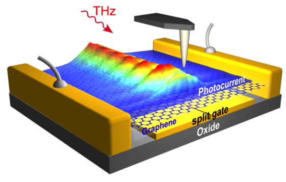
Now, researchers at CIC nanoGUNE (San Sebastian, Spain) in collaboration with ICFO (Barcelona, Spain), IIT (Genova, Italy) - members of the EU Graphene Flagship - Columbia University (New York, USA), Radboud University (Nijmegen, Netherlands), NIM (Tsukuba, Japan) and Neaspec (Martinsried, Germany) could visualize strongly compressed and confined THz plasmons in a room-temperature THz detector based on graphene. To see the plasmons, they recorded a nanoscale map of the photocurrent that the detector produced while a sharp metal tip was scanned across it. The tip had the function to focus the THz illumination to a spot size of about 50 nm, which is about 2000 times smaller than the illumination wavelength. This new imaging technique, named THz photocurrent nanoscopy, provides unprecedented possibilities for characterizing optoelectronic properties at THz frequencies.
The team recorded photocurrent images of the graphene detector, while it was illuminated with THz radiation of around 100 μm wavelength. The images showed photocurrent oscillations revealing that THz plasmons with a more than 50 times reduced wavelength were propagating in the device while producing a photocurrent.
“In the beginning we were quite surprised about the extremely short plasmon wavelength, as THz graphene plasmons are typically much less compressed”, says former nanoGUNE researcher Pablo Alonso, now at the University of Oviedo, and first author of the work. “We managed to solve the puzzle by theoretical studies, which showed that the plasmons couple with the metal gate below the graphene”, he continues. “This coupling leads to an additional compression of the plasmons and an extreme field confinement, which could open the door towards various detector and sensor applications”, adds Rainer Hillenbrand, Ikerbasque Research Professor and Nanooptics Group Leader at nanoGUNE who led the research. The plasmons also show a linear dispersion – that means that their energy is proportional to their momentum - which could be beneficial for information and communication technologies. The team also analysed the lifetime of the THz plasmons, which showed that the damping of THz plasmons is determined by the impurities in the graphene.
THz photocurrent nanoscopy relies on the strong photothermoelectric effect in graphene, which transforms heat generated by THz fields, including that of THz plasmons, into a current. In the future, the strong thermoelectric effect could be also applied for on-chip THz plasmon detection in graphene plasmonic circuits. The technique for THz photocurrent nanoimaging could find further application potential beyond plasmon imaging, for example, for studying the local THz optoelectronic properties of other 2D materials, classical 2D electron gases or semiconductor nanostructures.
CIC nanoGUNE receives 1.5 million euros from the European Commission

It is also worth highlighting that the European FET Open program is a highly competitive call given that out of the 902 projects submitted only 58 (6.6%) have been funded in the whole of Europe.
Funding for these three projects exceeds 1.5 million euros, of which €747,000 corresponds to the bioUPGRADE project, in which Raúl Pérez-Jimenez is participating; €390,625 is for the INTERFAST project, in which Luis Hueso is collaborating; and €375,000 goes to the SINFONIA project, in which Luis Hueso is also participating.
The nanoGUNE researchers assert that “the SINFONIA and INTERFAST projects are enabling us to go on exploring the properties of organic materials in the field of the most competitive electronics, and to bring our basic research proposals closer to commercial devices with the help of top companies”. Likewise, the BioUPGRADE project “enables biotechnology to be used to transform natural resources into a new generation of “high-tech” biomaterials”.
SINFONIA
The main aim of the SINFONIA project (Selectively activated INFOrmation technology by hybrid Organic Interfaces), coordinated by Luis Hueso, is to develop a technology that will allow information to be stored and transported on a nanometric scale operating in the ultra-rapid THz regime, beyond current conventional processors. SINFONIA is proposing a completely new approach to information technology.
BioUPGRADE
The BioUPGRADE (Biocatalytic upgrading of natural biopolymers for reassembly as multipurpose materials) project, coordinated by Raúl Pérez-Jiménez, brings together advances in genomics, protein engineering and materials science for the purpose of transforming the principal polymers in nature into high-performance biomaterials with numerous applications, ranging from energy to medicine.
INTERFAST
The INTERFAST (Gated INTERfaces for FAST information processing) project, coordinated by Luis Hueso, will be developing a novel technology platform to control the magnetic response of a material by means of electric pulses and thus propose new forms of ultra-dense information storage.
María Barra receives the Nanolito award for her Doctoral Thesis
The diplomas accrediting the Nanolito Doctoral Thesis Awards have been presented at the XXXIX Biennial of the Royal Spanish Society of Physics (RSEF), which is being held these days in Donostia San Sebastian. These awards seek to highlight the contribution of young scientists to the fields of nanolithography and nanofabrication, specifically those who have recently defended their doctoral thesis in Spain.
Summer Internship Program: call open until 5 February

NanoGUNE has just opened the registration period for the Summer Internship Program.
This year, we offer up to 13 projects for university students in the 3rd and 4th year of Physics, Chemistry, Biology, Engineering, and Mathematics. They will have the chance to get a closer look at the activity taking place at a cutting-edge research center for between six weeks and two months during the summer. This experience enables university students to collaborate with nanoGUNE researchers on their research projects in a whole range of fields, such as nanomagnetism, self-assembly, nanobiomechanics, nanodevices, nanomaterials, nanoimaging, and nanoengineering.
All the information about these projects, timetables, pay, etc. can be checked out at: https://www.nanogune.eu/summer-internship
Anyone interested in participated in the selection process needs to send an email attaching his/her academic record and CV to the address provided on the webpage no later than 5 February 2017. The students selected will be asked to attend an interview on 17 or 24 February.
CIC nanoGUNE collaborates with Intel to open up the way for future computers
According to the Ikerbasque researcher Fèlix Casanova, who is leading the “MESO” project at nanoGUNE, there are two unavoidable challenges that will drive the transition towards new electronic technologies. The first one, inherent to the current CMOS technology (based on silicon and used on a massive scale), is its physical limit. “The number of transistors integrated in a chip has been doubling every two years, but this scaling has a limit and when we make the transistor too small sometime soon, it will no longer work because we will lose ‘control’ over the electrons.
Unprecedented spin properties revealed in new artificial materials
In conjunction with research staff from the Charles University of Prague and the CFM (CSIC-UPV/EHU) center in San Sebastian, CIC nanoGUNE’s Nanodevices group has designed a new complex material with emerging properties in the field of spintronics.
ERC Proof of Concept for Luis Hueso

This project has its starting point in another previous one by the name of SPINTROS, which received 1.3 million euros through the ERC by means of the Starting Grant program; in it, new materials and functions were explored to design and develop new electronic devices based on organic semiconductors.
What the group wants to do now is to develop and market a prototype to measure the potential of organic molecules for electronic applications: FAST and Accurate Testing of Organic Material – FAST TestOM. “It is a small piece of equipment which will, for example, enable OLED screen producers to easily, rapidly, and economically measure the behavior of different organic molecules when emitting light,” explained Luis Hueso, leader of the Nanodevices Group.
The screens of many mobile phones are of the OLED (organic light-emitting diode) type. Its structure is based on a light-emitting layer consisting of a film of organic components that react to electric voltage by generating and emitting light on their own. According to the researcher, “this prototype would enable us to find out more easily and economically what type of organic molecule polymer will be able to emit more light, use less power, last longer, etc., with the resulting benefit for the production chain of commercial devices”.
Nanodevices Group in Nature Materials
September 2009, Volume 8 No 9 pp707-716
Spin routes in organic semiconductors
V. Alek Dediu (1), Luis E. Hueso (2), Ilaria Bergenti (1) & Carlo Taliani (1)
1. ISMN-CNR, via Gobetti 101, 40129 Bologna, Italy.
2. CIC nanoGUNE Consolider, Tolosa Hiribidea 76, E-20018 Donostia – San Sebastian and IKERBASQUE, Basque Foundation for Science, E-48011 Bilbao, Spain.
Correspondence to: V. Alek Dediu1 e-mail: V.Dediu@bo.ismn.cnr.it
The first-ever 2D spintronics device constructed entirely from proximitized structures
The field of spintronics has evolved significantly since the pioneering discoveries of spin injection and giant magnetoresistance in the 1980s, which relied on spin-polarized electron injection from a ferromagnetic metal to a normal metal. These groundbreaking achievements earned Albert Fert and Peter Grünberg the 2007 Nobel Prize in Physics, laying the foundation for ongoing research into complex material combinations and interface optimization techniques.
Magnetic electrodes increase solar cell efficiency
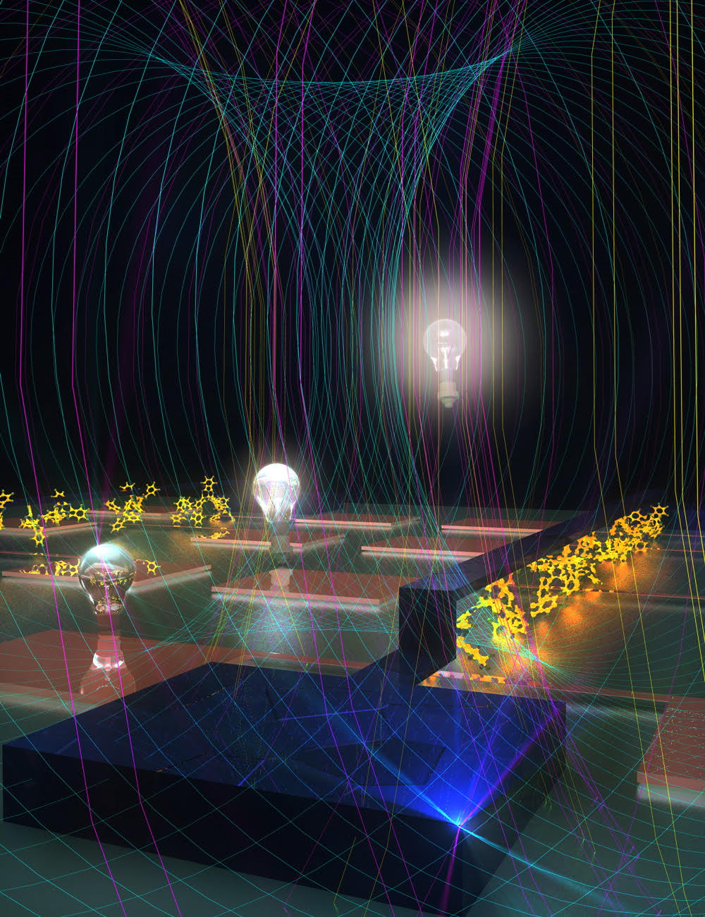
As the nanoGUNE researcher explained, “the device is simply a photovoltaic cell manufactured from an organic material —fullerene C60— and fitted with cobalt and nickel magnetic electrodes”. Fullerene C60, known as Buckyball, is a ball-shaped molecule comprising 60 carbon atoms. What is more, the magnetic electrodes produce current with an added property known as spin. The combination of both is no coincidence since fullerene is known to be a photovoltaic material that could allow the spin direction to be controlled. The use and control of this properly allows the efficiency of the solar cell to be increased, thus making it capable of generating a bigger current. As Hueso explained, “the spins of the usual solar cells are ‘disordered’ but thanks to magnetism we have managed to ‘order’ them so that a bigger current can be collected”. The researchers have confirmed that the use of electrodes of this type increases the photovoltaic efficiency of the device by 14%.
The device has another added advantage as it has been found to be capable of directly generating alternating current, which is much more useful in applications than the direct current generated by the usual solar cells, as transformers no longer need to be used. “The reversal of the current takes place in the device itself when the electrons created by the light interact with the magnetic contacts, whose spins have been ‘ordered’,” explained Hueso.
Even though it is true that the researchers have demonstrated that the use of magnetic electrodes allows the efficiency of the photovoltaic cells to be increased, they insist that they are still a long way from obtaining an optimum photovoltaic cell. With this aim in mind they are working on building similar devices using organic materials which have already shown themselves to be more efficient than fullerene. The researcher affirms that “in the future it will be possible to build a commercial device that acts as a solar module and produces alternating current directly”.
This work is the result of a piece of research funded by the Government of the Basque Autonomous Community, the Spanish Ministry for the Economy and Competitiveness, and the European Union through the European Research Council.
Fèlix Casanova receives the 2020 Intel Outstanding Researcher Award
Finding a replacement to current technology in electronics that can be smaller, faster and, most importantly, with less energy consumption is a global challenge. Fèlix Casanova and his team in nanoGUNE, in collaboration with the multinational company Intel, have been working hard in the last years in a disruptive technology for the electronics of the future: MESO technology. A new technology that combines memory, interconnects and logic requirements for future computing needs.
First year HINTS
The project HINTS, launched last 1st June 2011, has achieved its first year of life. The first results have been achieved and have been presented in Valencia, the 31st may 2012. The HINTS project, full title: “Next Generation Hybrid Interfaces for Spintronic Applications”, is funded with 3.87 million Euro granted by the European Commission in the 7th Framework Programme.
HINTS aims at advancing Spintronics by developing new hybrid organic-inorganic (HOI) materials featuring strong and tuneable spin-transfer efficiency at the interfaces. One of the main characteristics of all organic based ICT devices is the intrinsic hybrid combination of organic active materials with inorganic electrodes. Their greatest advantage is the possibility of low-cost processing and the enormous choice of molecules, most of which are still unexplored. Crucially most of the properties of the hybrids are determined by their interfaces so that the ability to tailor the degree of interaction between organic and inorganic materials impacts the functioning of entire devices and of the electronic properties of the composite materials in general.
The ambitious approach of HINTS is implemented by designing new materials with improved spin transfer efficiency and transport. HINTS will constantly benchmark the material parameters and properties with device demands. Thus the development and the selection of HOI materials will proceed in close collaboration with and with constant feedback from the industrial and SME partners, and the entire consortium will maintain awareness of the intermediate and final ICT needs (device aspects).
The project is developing hybrid materials which exhibit the following interface functionalities:
- controlled and well defined spin selectivity as a consequence of material combination;
- tuneable interface energy barriers for controlled charge and spin injection (dipole tailoring);
- spin scattering and spin control by the insertion of monolayers of high-spin-molecules at the interfaces;
- control of the non-linear interplay of charge and spin transfer and its use for multifunctional effects.
The project has now achieved the first year of life and this was characterized by a set of encouraging results among which we can mention:
- the achievement of strong GMR modulation via both proxity effect and electrical gating at spin injecting and collecting hybrid interfaces
- promissing preliminary results of SAM assisted TMR junctions
- extraordinary first observation of the GMR inversion in a GMR device via electrical field gating a
- first modification/adjustment of the technological tools (effusion cells) as required by the needs driven by HINTS objectives.
The HINTS project (full title: “Next Generation Hybrid Interfaces for Spintronic Applications”) is funded with 3.87 million Euro granted by the European Commission in the 7th Framework Programme, coordinated by Dr. Valentin Dediu of the Institute for the Study of Nanostructured Materials – ISMN (Italy), and carried out by a consortium of 14 leading research institutions coming from 8 Countries, each of them with specific roles and different levels of involvement. The consortium is composed by 7 Universities, 3 Research Centers and four companies spread across Europe.
The FP7 project HINTS started on the 1st of June 2011. The project held its kick-off meeting in Bologna (Italy), last 23rd – 24th June 2011.
Meeting on the digital future of Euskadi
The meeting on digital technologies took place on Friday, January 24 at the Ikerlan headquarters in Arrasate. At the meeting, organized by the Basque Research & Technology Alliance (BRTA) together with Ikerlan and Vicomtech, experts in digital technologies have shown the work being developed in the Basque Country.
CIC nanoGUNE is participating in two European projects to train young researchers
NanoGUNE recruits two early-stage researchers (ESRs) for the SPEAR project
Spin Orbitronics provides a challenging and innovative framework for training early-stage researchers with excellent prospects for a career in industry and academia. In this promising area, SPEAR proposes a multidisciplinary European network, composed of 7 universities, 3 research centers and 7 small and medium sized companies, which will provide state-of-the-art training for early-stage researchers (ESRs) in the field of fundamental and applied Spin Orbitronics.
Science: Flatland optics with graphene
Optical circuits and devices could make signal processing and computing much faster. “However, although light is very fast it needs too much space”, explains Rainer Hillenbrand, Ikerbasque Professor at nanoGUNE and the UPV/EHU. In fact, propagating light needs at least the space of half its wavelength, which is much larger than state-of-the-art electronic building blocks in our computers. For that reason, a quest for squeezing light to propagate it through nanoscale materials arises.
The wonder material graphene, a single layer of carbon atoms with extraordinary properties, has been proposed as one solution. The wavelength of light captured by a graphene layer can be strongly shortened by a factor of 10 to 100 compared to light propagating in free space. As a consequence, this light propagating along the graphene layer – called graphene plasmon – requires much less space.
However, transforming light efficiently into graphene plasmons and manipulating them with a compact device has been a major challenge. A team of researchers from nanoGUNE, ICFO and Graphenea – members of the EU Graphene Flagship – now demonstrates that the antenna concept of radio wave technology could be a promising solution. The team shows that a nanoscale metal rod on graphene (acting as an antenna for light) can capture infrared light and transform it into graphene plasmons, analogous to a radio antenna converting radio waves into electromagnetic waves in a metal cable.
“We introduce a versatile platform technology based on resonant optical antennas for launching and controlling of propagating graphene plasmons, which represents an essential step for the development of graphene plasmonic circuits”, says team leader Rainer Hillenbrand. Pablo Alonso-González, who performed the experiments at nanoGUNE, highlights some of the advantages offered by the antenna device: “the excitation of graphene plasmons is purely optical, the device is compact and the phase and wavefronts of the graphene plasmons can be directly controlled by geometrically tailoring the antennas. This is essential to develop applications based on focusing and guiding of light”.
The research team also performed theoretical studies. Alexey Nikitin, Ikerbasque Research Fellow at nanoGUNE, performed the calculations and explains that “according to theory, the operation of our device is very efficient, and all the future technological applications will essentially depend upon fabrication limitations and quality of graphene”.
Based on Nikitin´s calculations, nanoGUNE’s Nanodevices group fabricated gold nanoantennas on graphene provided by Graphenea. The Nanooptics group then used the Neaspec near-field microscope to image how infrared graphene plasmons are launched and propagate along the graphene layer. In the images, the researchers saw that, indeed, waves on graphene propagate away from the antenna, like waves on a water surface when a stone is thrown in.
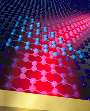
Graphic representation of the refraction of graphene plasmons – launched by a tiny gold antenna – when passing through a one-atom-thick prism
In order to test whether the two-dimensional propagation of light waves along a one-atom-thick carbon layer follow the laws of conventional optics, the researchers tried to focus and refract the waves. For the focusing experiment, they curved the antenna. The images then showed that the graphene plasmons focus away from the antenna, similar to the light beam that is concentrated with a lens or concave mirror.
The team also observed that graphene plasmons refract (bend) when they pass through a prism-shaped graphene bilayer, analogous to the bending of a light beam passing through a glass prism. “The big difference is that the graphene prism is only two atoms thick. It is the thinnest refracting optical prism ever”, says Rainer Hillenbrand. Intriguingly, the graphene plasmons are bent because the conductivity in the two-atom-thick prism is larger than in the surrounding one-atom-thick layer. In the future, such conductivity changes in graphene could be also generated by simple electronic means, allowing for highly efficient electric control of refraction, among others for steering applications.
Altogether, the experiments show that the fundamental and most important principles of conventional optics also apply for graphene plasmons, in other words, squeezed light propagating along a one-atom-thick layer of carbon atoms. Future developments based on these results could lead to extremely miniaturized optical circuits and devices that could be useful for sensing and computing, among other applications.
Original publication
P. Alonso-González1, A.Y. Nikitin1,5, F. Golmar1,2, A. Centeno3, A. Pesquera3, S. Vélez1, J. Chen1, G. Navickaite4, F. Koppens4<, A. Zurutuza3, F. Casanova 1,5, L.E. Hueso 1,5 and R. Hillenbrand 1,5. “Controlling grapheme plasmons with resonant metal antennas and spatial conductivity patterns” Science (2014), DOI: 10.1126/science.1253202
- CIC nanoGUNE, 20018 Donostia-San Sebastián, Spain.
- I.N.T.I-CONICET and ECyT-UNSAM, San Martín, Bs. As., Argentina.
- Graphenea SA, 20018 Donostia-San Sebastián, Spain.
- ICFO-Institut de Ciéncies Fotoniques, Mediterranean Technology Park, 08860 Casteldefells, Barcelona, Spain.
- IKERBASQUE, Basque Foundation for Science, 48011 Bilbao, Spain.
CIC nanoGUNE
The nanoGUNE Cooperative Research Center, located in Donostia-San Sebastian, Basque Country, is a research centre set up with the mission to conduct excellence research into nanoscience and nanotechnology with the aim of increasing the Basque Country’s business competitiveness and economic and social development.
GRAPHENEA S.A.
Graphenea is a pioneer graphene production start-up company founded in 2010 by private investors and CIC nanoGUNE. The company produces and commercializes graphene films by Chemical Vapor Deposition technology and graphene powders by Chemical Exfoliation techniques.
ICFO
ICFO is a young research institution located in Barcelona that aims to advance the very limits of knowledge in Photonics, namely the science and technology of harnessing Light. Its research programs target the global forefront of photonics, and aim to tackle important challenges faced by society at large. ICFO is focused on current and future problems in Health, Energy, Information, Safety, Security and caring for the Environment.
Donostia, the spintronics and orbitronics capital
Donostia has become the epicenter of research in spintronics and orbitronics this week with the celebration of Spin & Orbit at the Gipuzkoa Campus of the University of the Basque Country, a conference that brings together world experts in these innovative fields of physics, crucial for the development of the electronics of the future.
Basque researchers turn light upside down
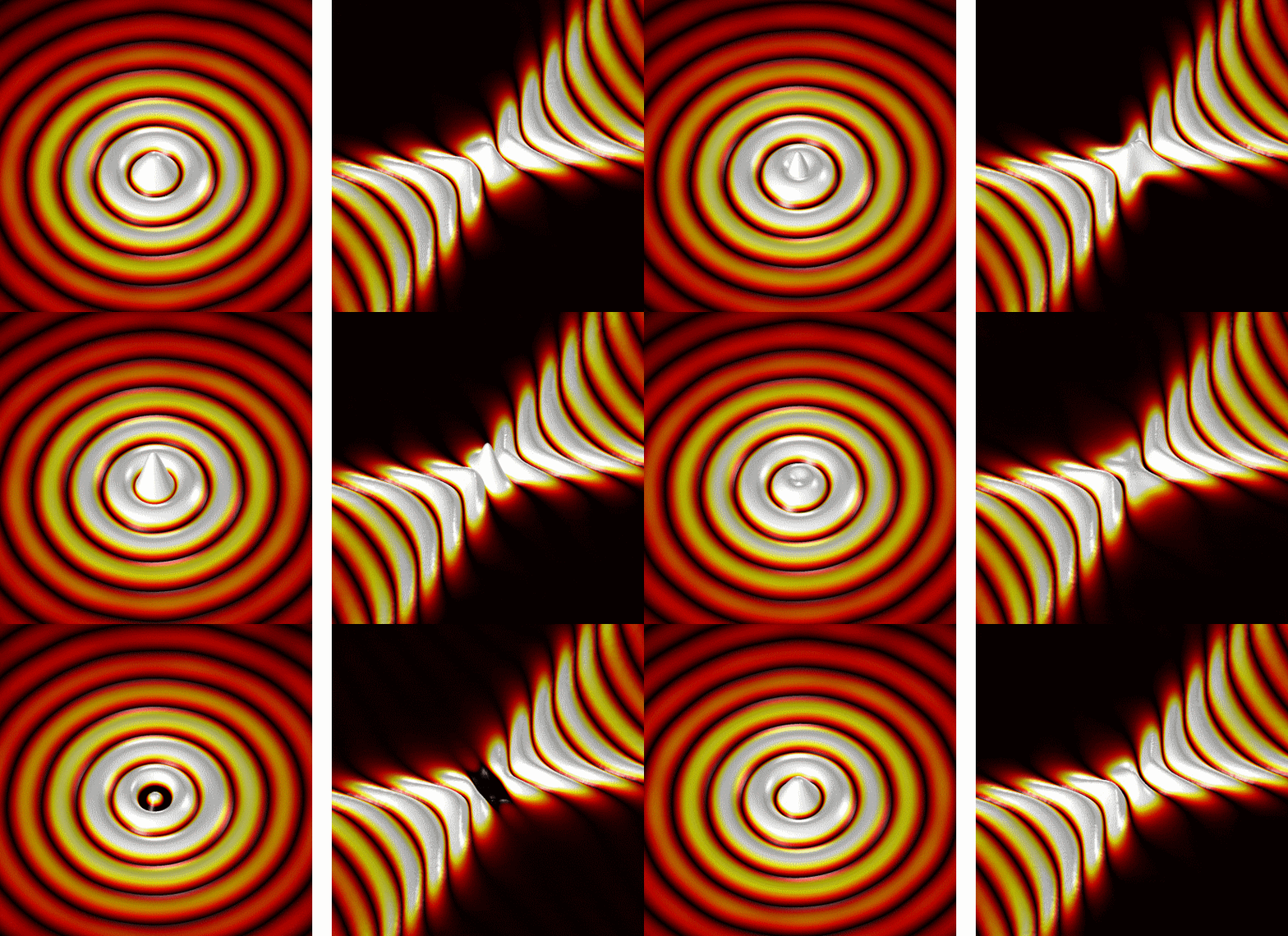
Scientists had already theoretically predicted that specifically structured surfaces can turn the wavefronts of light upside down when it propagates along them. "On such surfaces, called hyberbolic metasurfaces, the waves emitted from a point source propagate only in certain directions and with open (concave) wavefronts", explains Javier Alfaro, PhD student at nanoGUNE and co-author of the paper. These unusual waves are called hyperbolic surface polaritons. Because they propagate only in certain directions, and with wavelengths that are much smaller than that of light in free space or standard waveguides, they could help to miniaturize optical devices for sensing and signal processing.
Now, the researchers developed such a metasurface for infrared light. It is based on boron nitride, a graphene-like 2D material, and was selected because of its capability to manipulate infrared light on extremely small length scales, which could be applied for the development of miniaturized chemical sensors or for heat management in nanoscale optoelectronic devices. On the other hand, the researchers succeeded to directly observe the concave wavefronts with a special optical microscope, which have been elusive so far.
Hyperbolic metasurfaces are challenging to fabricate because an extremely precise structuring on the nanometer scale is required. Irene Dolado, PhD student at nanoGUNE, and Saül Vélez, former postdoctoral researcher at nanoGUNE (now at ETH Zürich) mastered this challenge by electron beam lithography and etching of thin flakes of high-quality boron nitride provided by Kansas State University. "After several optimization steps, we achieved the required precision and obtained grating structures with gap sizes as small as 25 nm”, Dolado says. “The same fabrication methods can also be applied to other materials, which could pave the way to realize artificial metasurface structures with custom-made optical properties”, adds Saül Vélez.
To see how the waves propagate along the metasurface, the researchers used a state-of the-art infrared nanoimaging technique that was pioneered by the nanoptics group at nanoGUNE. They first placed an infrared gold nanorod onto the metasurface. “It plays the role of a stone dropped into water”, says Peining Li. The nanorod concentrates incident infrared light into a tiny spot, which launches waves that then propagate along the metasurface. With the help of a so-called scattering-type scanning near-field microscope (s-SNOM) the researchers imaged the waves. “It was amazing to see the images. They indeed showed the concave curvature of the wavefronts that were propagating away form the gold nanorod, exactly as predicted by theory“, says Rainer Hillenbrand, Ikerbasque Professor at nanoGUNE, who led the work.
The results promise nanostructured 2D materials to become a novel platform for hyberbolic metasurface devices and circuits, and further demonstrate how near-field microscopy can be applied to unveil exotic optical phenomena in anisotropic materials and for verifying new metasurface design principles.
The research has been mainly funded by individual fellowship grants of the European Union Marie Sklodowsca-Curie Actions and the pre-doctoral research grants program of the Basque and Spanish Governments, as well as by the National Science Foundation (USA), and has been carried out in line with nanoGUNEs projects within the EU's Graphene Flagship.
Spin Control Without Magnetic Fields
In graphene, spin currents can live much longer than they can in other materials, making the material an ideal platform for future spintronic devices. But there is a problem: To manipulate graphene’s spin currents, researchers need to apply a magnetic field to the material. The necessary hardware is difficult to integrate into circuits, limiting how small graphene-based spin devices could be shrunk.
Marco Gobi, Best Experimental Thesis Award
The GEFES awards ceremony will take place on July 2015, during their symposium on the 25th Spanish Royal Physical Society’s Biannual meeting in Gijón (Spain). Alejandro Manjavacas, who developed his PhD thesis at the "Rocasolano" Institute of Physical-Chemistry, has been awarded the Best Theorical Thesis prize for his thesis project: “Light-matter interaction at the nanoscale”.
Marco Gobbi’s thesis describes the fabrication and characterization of spintronic devices based on the combination between thin films of ferromagnetic metals and C60 fullerene molecules. Then, he focuses on two spintronic devices based on C60: spin valves and magnetic tunnel transistors. He concludes with the description of a device for more advanced study of spin transport in C60.
Sofia Ferreira Teixeira receives the Inspira Gazteak 2025 Award
Sofia, a MSCA fellow researcher at CIC nanoGUNE, was recognized for her outstanding career in scientific research and outreach, becoming a role model for younger generations. The award, which includes a €15,000 prize, will support her continued work with increased visibility and impact.
At nanoGUNE, we warmly congratulate Sofia on this well-deserved recognition and celebrate her contribution to advancing knowledge and inspiring future scientists.
Students from UPV / EHU, Tecnun, UAB and the UB carry out summer internships at CIC nanoGUNE
On Tuesday, 19 June, we welcomed a group of internship students that will carry out a research project at NanoGUNE during the summer. The director of the center, Jose M. Pitarke, received the students with a presentation talk about nanoGUNE, that was also attended by the researchers that will conduct the students’ projects.
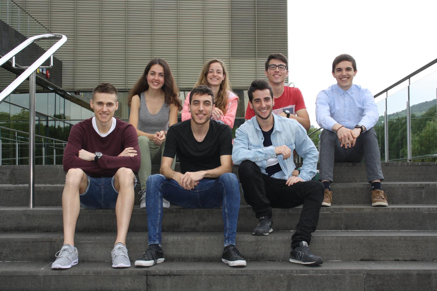
The 11 students come from different universities, among which are, Unibersity of the Basque Country (UPV /EHU), Tecnun, Univeristy of Barcelona (UB), Autonomous University of Barcelona (UAB). This program offers to the students a real experience of work in a research laboratory in order to make it easier for them to take decision about their future professional life.
The students will collaborate and learn with the different research groups at nanoGUNE, such as nanooptics, nanodevices or nanomagnetism. They will carry out a research project for two months following the instructions of a researcher of their group.
Some of them started the internships at the beginning of the month and they have been very involved in the group’s work. "The truth is that we started very suddenly; the very first day they took me to the laboratory," says Amaia Ochandorena, a student of Biochemistry and Molecular Biology at the UPV/EHU.
All the students knew CIC nanoGUNE and stressed that "it is an important research center" and "offers and works with topics of much interest".
For these students, and also for undergraduate students of general, nanoGUNE offers the possibility of collaborating with the center for the completion of final graduate or master thesis projects, for which also opens a call for grants every year.
Registration period for the summer internship program open
CIC nanoGUNE has just launched the program for summer internships, which runs every year. University students are offered the chance to get involved in the activity of a world-class research center.
The researcher Estitxu Villamor got a special mention in the CAF-Elhuyar awards
Among the various categories and subcategories in the awards there is one of popularization articles based on PhD theses. In fact, Estitxu Villamor got the special mention for her article entitled "Karga-garraiorik gabeko elektronika berria" (New electronics without charge transport). The panel of judges felt that the following was worthy of mention: "The effort made by the author of the article to explain the subject in an easy-to-understand and attractive way, particularly bearing in mind that it is a highly technical subject".
Villamor defended her thesis entitled Injection, transport and manipulation of pure spin currents in metallic lateral spin valves in December 2014.
Beatriz Martín García receives one of the 2025 Journal of Materials Chemistry Lectureship runner-up awards
The Journal of Materials Chemistry, a prestigious publication of the Royal Society of Chemistry (RSC), established in 2016 an annual lectureship together with two runners-up awards, which intend to recognize the achievements of early-career scientists and acknowledges their significant contributions to the field of materials chemistry.
Edurne Sagasta, winner of the GEFES 2019 Award for best experimental thesis
This thesis explores the Hall spin effect, an effect that takes place in metals with spin-orbit coupling and allows charge currents to be converted into spin currents and vice versa. These conversions are of huge technological interest as they have the potential for use in the process to write magnetic memories (like MRAMs) and to read them (as in spin-based log circuits, a recent proposal by Intel). This research has revealed the mechanisms that contribute towards this effect in certain metals, such as platinum (Pt) or tantalum (Ta), which has made it possible to show how the efficiency of this conversion can be enhanced. Platinum (Pt) has also been combined with graphene to produce a device that can efficiently convert spin currents into charge ones.
The Hall spin effect is related to the anomalous Hall effect, known since the 19th century but little understood until recently. The second part of the thesis shows that this relationship in ferromagnetic materials is more complex than previously thought.
Edurne Sagasta
Edurne Sagasta studied physics at the UPV/EHU-University of the Basque Country and after getting a Master’s degree in Nanoscience and Advanced Materials at the same university, she started her PhD thesis at nanoGUNE. ”After studying Physics at university, I wanted to do something that would be more practical. At the same time, I wanted to get involved in a project with more people and have the chance to visit different labs across the world; in short, to embark on a research project,” said the researcher. "Once I had finished my PhD, I decided to make the leap to the world of industry, and right now I am working for the company Mondragon Assembly,” she said.
Fèlix Casanova receives the Intel Outstanding Researcher Award for the second time
Finding a replacement for today’s electronic technology to make it smaller, faster and, most importantly, more energy-efficient, i.e. so that it consumes less, is a global challenge. In recent years, Fèlix Casanova and his nanoGUNE team have been working in collaboration with the multinational Intel on a research project aimed at improving the performance and energy savings of future computers by optimizing MESO technology.
nanoGUNE Scholarship: call for Master Thesis students
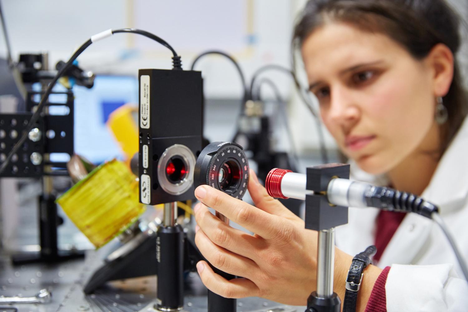
The Scholarships will be of a total amount of 3,000€. This amount is for the whole period and will not be compatible with any other grant or funding awarded for the same purpose. Candidates have to be pre-registered and accepted at the above mentioned Master degrees in order to be eligible for these grants. Interested candidates can find all the information about the offered master projects and the application process following this link.
Besides the grants, nanoGUNE offers Master students coming from any official Master degree the possibility to develop their Master Thesis within one of its research groups.
nanoGUNE launches a new summer internship call for university students
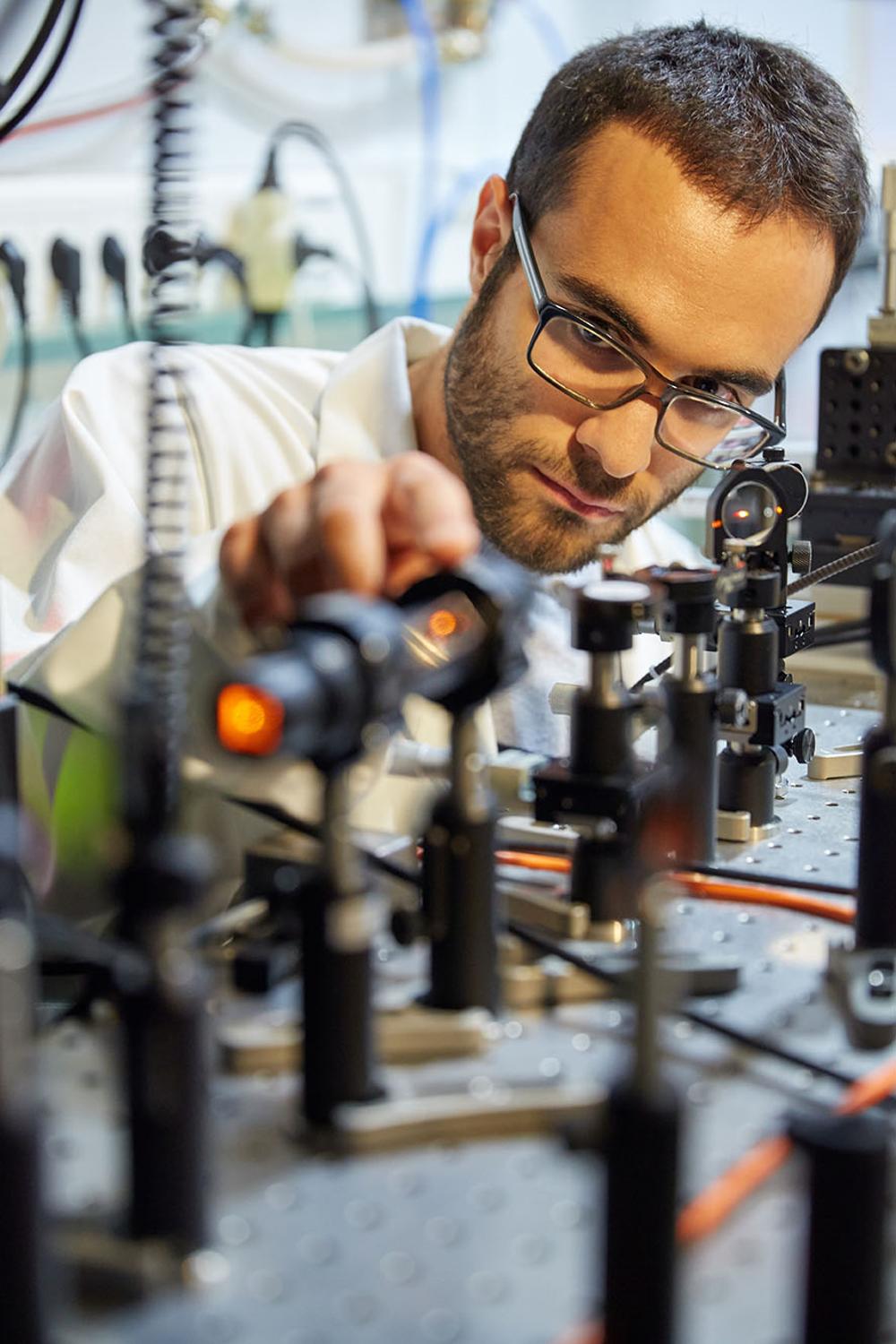
Through this programme the Basque nanoscience research centre will this summer be receiving about ten new students in their 3rd and 4th years of Physics, Chemistry, Biology and Engineering. For a period of six weeks or two months the young students will be collaborating with nanoGUNE researchers in their research projects on subjects such as electron/spin phenomena and magnetism, nanoscale optics, nanoscale materials and nanobioengineering, among others.
To participate in the summer internship programme any students who are interested will need to submit their applications online via the nanoGUNE website, the deadline being 16 February. Full information relating to the call is available via the nanoGUNE website (www.nanogune.eu)
The building block for magnetoelectric spin-orbit logic
A pathway for magnetic-field-free, voltage-based switching of magnetism has been proposed using magnetoelectric materials that exhibit more than one of the primary ferroic properties in the same phase.

