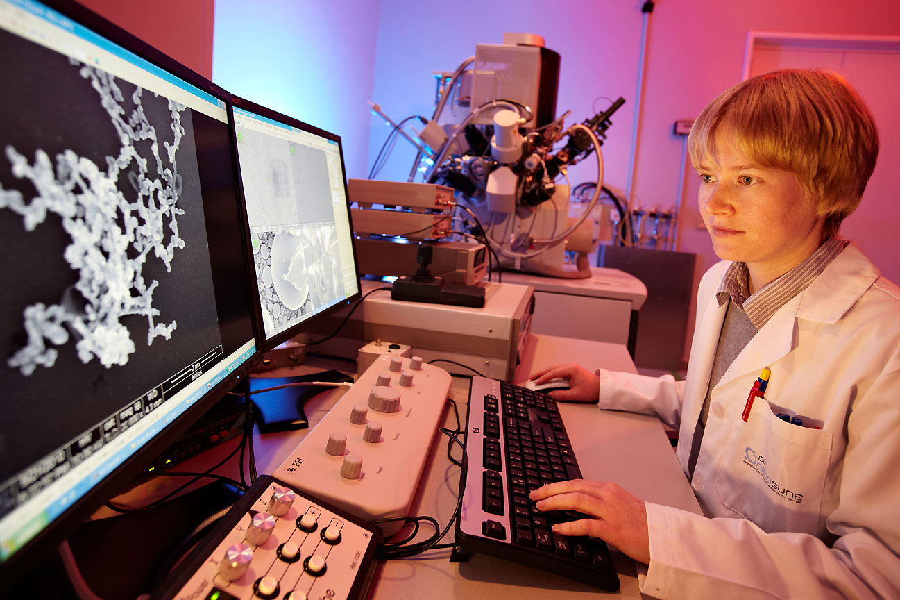
Dual-beam FIB/SEM (Focused Ion Beam and Induced deposition)
Offered as External Service
Focused Ion Beam (FIB) and Focused electron/ion beam induced deposition (FE(I)BID), system used for surface patterning and complex structures fabrication.
Research group
Technical characteristics
- High tension electron column 50 V - 30 kV
- High tension Ga-column 0.5 kV – 30 kV
- Electron column resolution 0.5 nm at 15 kV and 0.8 nm at 1 kV (STEM)
- FIB milling resolution 10 nm at 30 kV
- GIS percursor for FE(I)BID: platinum, silicon oxide, gold, tungsten, cobalt
- Nanomanipulator with microgripper (Kleindiek)
- LN2 cooling stage (CryoMat )
- EDX silicon drift detectors for elemental analysis (EDAX)
- Detectors: ETD SE, True in-Lens Detector (TLD), STEM II detector, High performance Ion Conversion and Electron (ICE), Concentric Back Scatter (CBS) detector
- iFast software for advanced Dual Beam automation in order to automate the imaging and nanofabrication
- MAPSTM for automatic acquisition of extra large images with high resolution
- AutoSlice&ViewTM software for 3D imaging by sequential sectioning of the sample
Equipment
Cleanroom
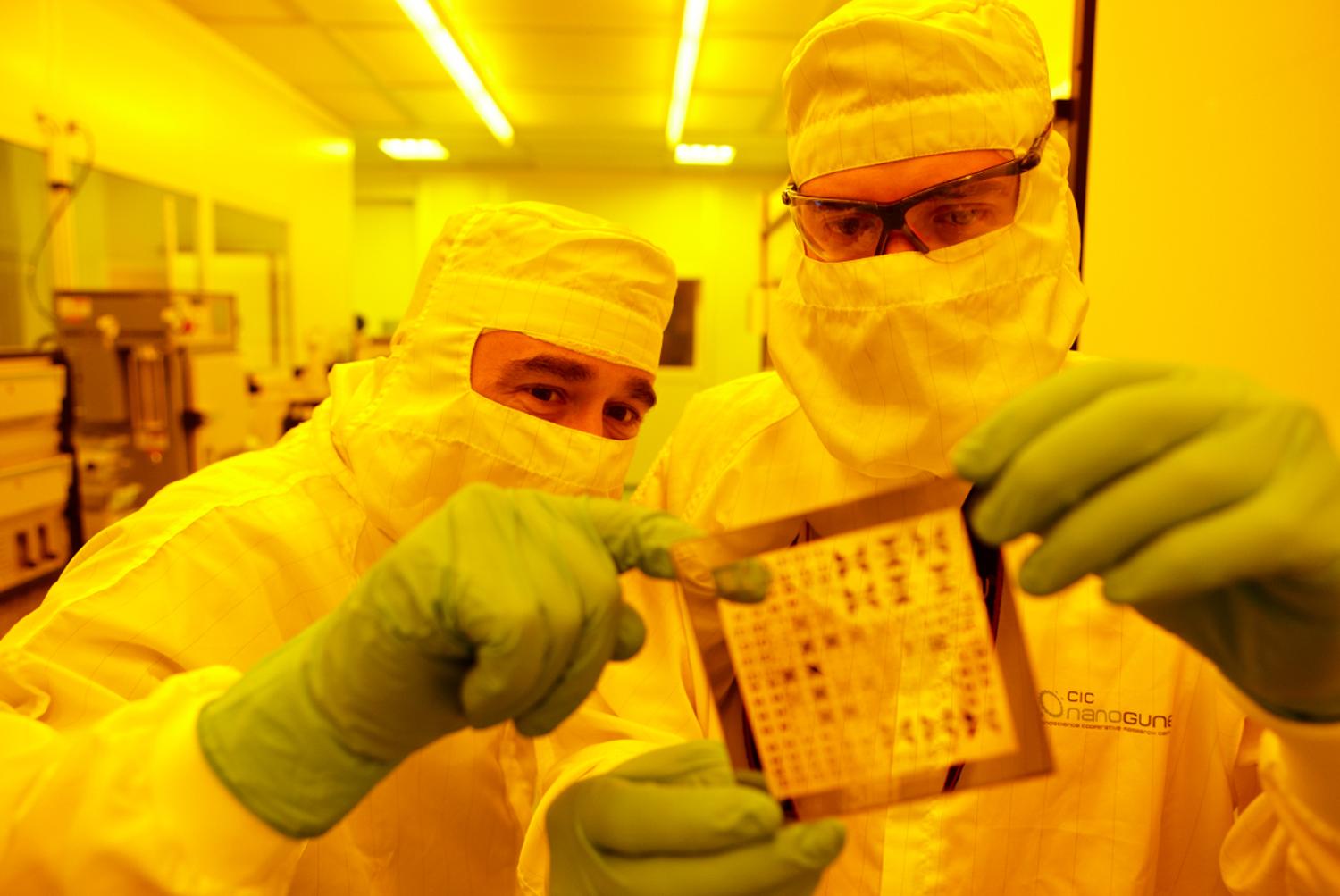
The nanoGUNE cleanroom, dedicated to fabricate and characterize the properties of materials on the nanoscale, ia a 300m2 laboratory where the air purity is under strict supervision.
Equipment
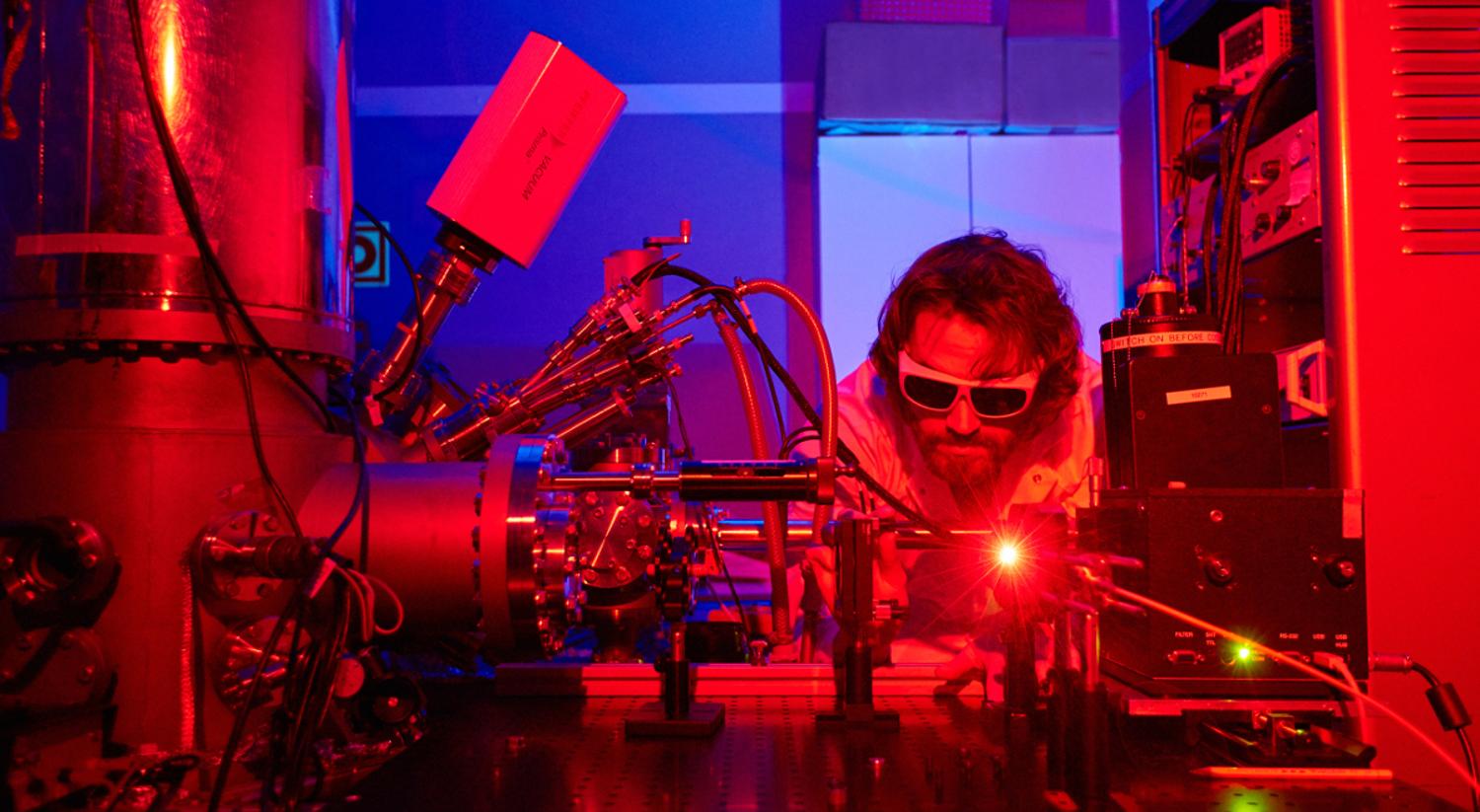
State-of-the-art equipment, including electron and scanning-tunneling microscopes, as well as other nanofabrication and characterization tools, are managed by specialists and used by researchers from a wide variety of fields.